
High Density Interconnect (HDI) PCB Design Explained: Worth It?
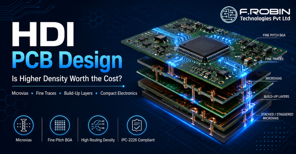
High density interconnect (HDI) PCB design packs more circuitry into less space than a conventional board, using microvias, finer traces, and tighter spacing. As electronics shrink and components grow more complex, HDI has moved from a niche option to a mainstream necessity. But it also costs more — so the real question is whether high-density design is worth it for your product. This guide explains HDI PCB design in plain terms: what it is, the key technologies behind it, when it pays off, and the design rules that keep it reliable. Whether you are designing a compact wearable or a dense processor board, you will learn when a high density interconnect approach is the right call. What Is HDI PCB Design? High density interconnect PCB design is an approach that achieves higher wiring density than standard boards through microvias, fine lines, and thin build-up layers. In short, it lets you route far more connections in the same area — or fit the same circuit into a much smaller board. An HDI circuit board uses laser-drilled microvias instead of large mechanically drilled holes, along with finer traces and tighter spacing. These features free up routing space that conventional vias would block. As a result, a high density interconnect PCB can support today’s fine-pitch components, which a standard board often cannot. HDI is defined by IPC-2226, which classifies designs into types based on their build-up structure. The common thread is the same: more connections, smaller features, and a board built up in layers rather than drilled all at once. HDI vs Standard PCB Design The difference between HDI and a standard board comes down to density and how the board is built. A conventional PCB is drilled and plated in a single pass with through-hole vias. A high density interconnect PCB is built up in stages, adding thin layers with microvias between them. This staged construction unlocks much greater density. Where a standard board hits a routing wall, HDI keeps going — fanning out hundreds of pins from a fine-pitch BGA that through-holes could never escape. The trade-off is added cost and manufacturing complexity, which we cover below. For designs that are not space-constrained, a conventional multilayer PCB usually offers better value. HDI earns its place only when density genuinely demands it. Key HDI Technologies Several technologies make high density interconnect design possible. Understanding them clarifies what HDI actually involves. These work together to escape dense components. A fine-pitch BGA, for example, may need via-in-pad and stacked microvias just to break out every signal. For a closer look at the via economics, see our guide to blind and buried vias. When Does HDI Pay Off? High density interconnect design pays off when density, size, or performance demands exceed what a standard board can deliver. It is worth the investment when: In these cases, a high density interconnect approach is not optional — the product could not exist, or would be far larger, without it. That is when the extra cost is clearly justified. HDI Design Rules Reliable high density interconnect boards follow a set of core design rules. Respecting them keeps the board manufacturable and robust. Following these rules — and the IPC-2226 standard — prevents the most common HDI failures. Designing within your manufacturer’s stated capabilities is just as important as the rules themselves. HDI Build-Up Types (IPC-2226) IPC-2226 classifies high density interconnect boards by their build-up structure, which helps you and your fabricator agree on complexity: As the type number rises, so does density — and cost. Choosing the lowest type that meets your routing needs is the single biggest lever for keeping an HDI board affordable. Discuss the target type with your fabricator before you finalize the stack-up, since it shapes every later decision. Cost Considerations HDI costs more than standard PCB design, mainly because of how it is built. Sequential lamination, laser drilling, and tighter tolerances each add process steps, time, and inspection. As a rule, every added build-up layer or lamination cycle raises cost. So the smart approach is to use the minimum HDI complexity that meets your needs — not the most advanced structure available. A clean handoff to PCB manufacturing keeps those costs predictable, and your fabricator can advise which HDI type balances density and price for your board. Best Practices for HDI Design Apply these practices to get the most from a high density interconnect design: Sound HDI design balances density, reliability, and cost. Working with experienced PCB layout design services helps you adopt only the high density interconnect features your product truly requires. Common Mistakes to Avoid Even capable teams trip up on HDI. Watch for these: Avoiding these keeps your high density interconnect board reliable, manufacturable, and on budget. Key Takeaways Conclusion HDI PCB design is worth it when your product’s density, size, or performance demands exceed what a standard board can deliver — fine-pitch BGAs, tight spaces, high layer counts, or high-speed signals. A high density interconnect approach uses microvias, via-in-pad, and build-up layers to achieve that density, at higher cost. The key is matching the HDI complexity to your real needs and following IPC-2226 design rules. Need HDI for Your PCB Design? Wondering whether your board really needs High Density Interconnect (HDI)? Our PCB layout design services help you adopt only the HDI features your design truly require—balancing routing density, reliability, manufacturability, and cost. Talk to Our Engineering Team → Frequently Asked Questions 1. What is HDI PCB design? HDI (High Density Interconnect) PCB design achieves higher wiring density than standard boards using microvias, fine traces, and thin build-up layers, allowing more connections in less space. 2. What is a high density interconnect PCB? A high density interconnect PCB is a board built with laser-drilled microvias, fine traces, and sequential build-up layers to support fine-pitch components and compact electronic designs. 3. What is the difference between HDI and a standard PCB? A standard PCB primarily uses through-hole vias, whereas an HDI PCB uses microvias, finer traces, and advanced layer
Custom PCB Design Services: When Off-the-Shelf Won’t Cut It
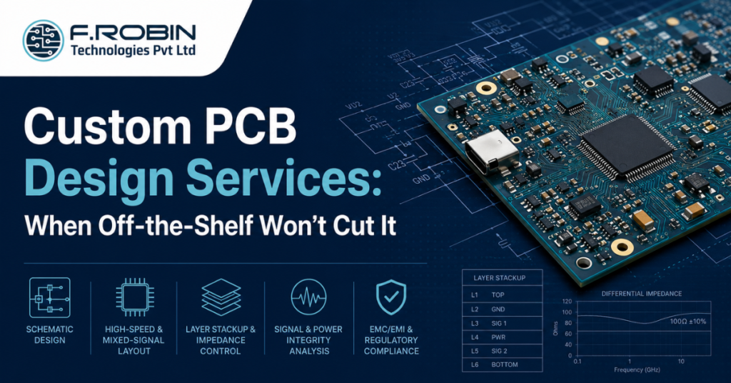
There is a moment in every hardware product cycle when a development module stops being a solution and starts being a constraint. The form factor is wrong. Unit costs are eroding margin. The RF noise is killing your analog front end. Your certification lab just handed back a failure report. That moment is when custom PCB design services become the only logical path forward. This guide helps hardware engineers, product managers, and procurement leads decide when to move from commercial modules to a purpose-built electronic PCB design — and what a professional engagement actually involves. What Are Custom PCB Design Services? Custom PCB design services are the end-to-end engineering process of designing a printed circuit board from the ground up — tailored to your product’s exact electrical, mechanical, thermal, and regulatory requirements. A professional PCB design company typically delivers: Custom electronic PCB design is not always necessary. But when it is, the gains in performance, size, cost, and certification compliance are difficult to achieve any other way. Off-the-Shelf vs. Custom PCB Design: Direct Comparison Factor Off-the-Shelf Module Custom PCB Design Time to Prototype Days to weeks 4–12 weeks NRE Cost None Moderate to high Unit Cost at Volume High (module premium) Low (optimized BOM) Form Factor Control Fixed Full control Regulatory Certification Often pre-certified Requires own testing IP Protection Low High proprietary design Mixed-Signal Performance Compromised Fully optimized Long-Term Supply Risk Module discontinuation Component-level sourcing Bottom line: For prototypes or low-volume internal tools, commercial modules are often the right call. For production-bound, certification-required, or cost-sensitive products, custom PCB design services pay for themselves. 7 Signs You Need Custom PCB Design Services 1. Your Form Factor Is Fixed and Modules Don’t Fit Medical wearables, aerospace enclosures, industrial handheld instruments — these have non-negotiable physical envelopes. When no commercial module fits, a custom PCB designed to exact mechanical constraints is the only option. 2. You’re Paying Module Premium at Production Volume Modules are priced for flexibility and small quantities. At 5,000+ units annually, the per-unit cost premium typically exceeds the original NRE investment within 12–18 months. 3. Your Design Has High-Speed Digital Signals Above 100 MHz — or with interfaces like DDR4, PCIe, USB 3.x, or MIPI — impedance-controlled routing and proper layer stackup are non-negotiable. These requirements demand high-speed digital and mixed-signal PCB layout expertise that commercial modules cannot substitute. 4. You’re Mixing Analog and Digital Domains Mixed-signal PCB design is among the most demanding disciplines in electronic PCB design. Poor ground plane management or insufficient isolation between analog and digital sections can destroy ADC performance or cause EMI failures. 5. Your Product Must Pass Regulatory Certification FCC Part 15, CE marking, IEC 60601 — certification evaluates the entire assembly. A PCB designed with EMC compliance in mind (shielding zones, controlled impedance, ferrite placement) has a significantly higher first-pass compliance rate. 6. You Have a Supply Chain or IP Concern Module vendors can discontinue products or become sole-source dependencies. Custom PCB design distributes sourcing risk across multiple suppliers and protects your architecture as proprietary IP. 7. Your Product Competes on Performance If your market position depends on a lower noise floor, faster processing, tighter latency, or higher precision, every compromised trace and shared power rail is a competitive liability. Custom PCB design services exist to remove these compromises. What Professional PCB Design Services Include Engaging a qualified PCB design company delivers more than a routed layout file. A full engagement covers: Schematic Capture and Review The design process starts with a verified schematic. The PCB design team reviews all reference designs, application notes, and datasheet recommendations. Errors caught here cost a fraction of what they cost after fabrication. Layer Stackup and Impedance Planning For high-speed or RF designs, the stackup is engineered before a single trace is routed. Layer count, dielectric material, copper weights, and layer assignments determine whether controlled impedance targets (50Ω single-ended, 100Ω differential) are achievable. Component Placement and Routing Experienced PCB designers apply thermal management, signal integrity, and DFM principles simultaneously during placement and routing. High-speed nets require length matching, guard routing, and verified return path continuity. DFM Review and Gerber Output A complete deliverable package includes fabrication-ready Gerber files, drill files, a BOM with approved alternates, assembly drawings, and a fabrication specification. High-Speed Digital and Mixed-Signal PCB Layout: Why It Matters High-speed digital and mixed-signal PCB layout combines signal integrity engineering, EMC design, and analog circuit principles — and is where most first-time custom PCB projects encounter problems. Key principles every PCB design company should apply: A poorly routed DDR5 interface can cause data corruption at speed. A shared ground between a switching regulator and a low-noise amplifier can inject hundreds of millivolts of noise into your signal chain. These are not edge cases — they’re common failure modes in designs that skip specialist mixed-signal PCB layout review. Key Takeaways Ready to Move from Module to Custom? If a commercial module is limiting your product’s performance, inflating costs, or blocking certification, it’s time to work with a PCB design team that understands the full engineering picture. Request a Design Consultation →
Multilayer PCB Design: How Many Layers Do You Really Need?
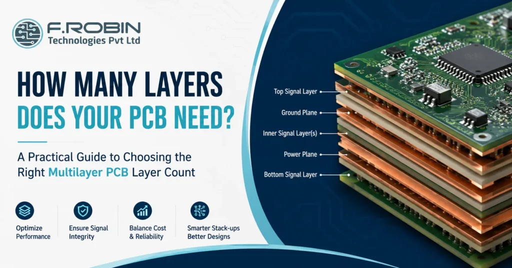
Choosing the right multilayer PCB layer count is one of the most consequential decisions in any hardware project. Pick too few layers and you fight routing congestion, noise, and signal problems. Pick too many and you inflate cost for no real benefit. So how many layers do you really need? The short answer: most products land on 4 layers, but the right number depends on signal speed, routing density, power complexity, and budget. In this decision guide, we walk through a practical framework for sizing a multilayer PCB, share common stack-up configurations, and show where the cost-versus-performance line really sits. By the end, you will be able to justify your layer count with confidence. What Is a Multilayer PCB? A multilayer PCB is a circuit board with three or more conductive copper layers separated by insulating material and bonded into a single board. Unlike a single- or double-sided board, a multilayer circuit board stacks signal layers, power planes, and ground planes vertically to pack more connections into less space. These extra layers do two important jobs. First, they give you more room to route dense designs. Second, dedicated power/ground planes deliver cleaner power and shorter return paths, which improves signal quality and reduces noise. Consequently, almost every modern product — from a smartphone to an industrial controller — relies on multilayer PCB design. The term layer stack (or stack-up) describes exactly how those layers are arranged. Getting the layer stack right is the heart of good multilayer PCB design, because it sets impedance, return paths, and manufacturability all at once. Why Layer Count Matters Layer count is not just a routing detail — it shapes performance, cost, and reliability together. Because each pair of layers adds material and process steps, every extra layer increases the price of your multilayer circuit board. Therefore, you want the lowest layer count that still meets your electrical goals. More layers deliver clear advantages: However, the benefits taper off. Adding layers a design does not need wastes money and lengthens lead times. As a result, smart multilayer PCB design is a balancing act enough layers to perform well, but no more than necessary. How Many Layers Do You Really Need? Use this framework to size your multilayer PCB. Work through the factors first, then match them to the layer-count guide below. Step 1: Assess the Key Factors Five factors drive layer count: Step 2: Match Factors to a Layer Count Layers Best For What You Get 2 Simple, low-speed, cost-sensitive boards Signal routing on both sides; no dedicated power or ground planes 4 Most products Two signal layers plus dedicated power and ground planes 6 Moderately complex designs with some high-speed nets Additional signal layers with multiple reference planes 8 High-speed digital designs and dense routing Strong impedance control, improved signal integrity, and isolation 10–16+ Multi-layer multi-processor board design, HDI, telecom systems Maximum routing density, multiple planes, shielding, and performance Step 3: Add a Margin If your design sits on the edge between two counts, choose the higher one. A single respin to add layers costs far more than the modest material premium of starting with enough. This is especially true for high-speed work, where you can also pair the layout with signal integrity analysis to confirm the stack-up performs as intended. Common Multilayer PCB Stack-Up Configurations The way you arrange signal layers and power/ground planes matters as much as the layer count. Here are proven layer stack patterns. 4-Layer Stack-Up A classic 4-layer multi layer pcb board uses: Signal – Ground – Power – Signal. The ground plane sits directly under the top signal layer, giving high-speed traces a clean return path. This arrangement suits the majority of products. 6-Layer Stack-Up A common 6-layer layer stack is: Signal – Ground – Signal – Signal – Power – Signal. It adds two more routing layers while keeping references close to critical signals. Use it when a 4-layer board runs out of room or needs better isolation. 8-Layer and Beyond High-speed and multi-layer multi-processor board design often needs 8 or more layers to provide multiple ground and power planes between signal layers. This sandwiching maximizes shielding and impedance control. As density climbs, HDI techniques and blind/buried vias frequently join the stack. PCB Design Tip Rule of thumb: Every signal layer should sit adjacent to a reference plane. If it does not, revisit your layer stack. Keeping signal layers next to ground or power planes improves return-current paths, impedance control, signal integrity, and EMI performance. Cost vs Performance: The Multilayer PCB Trade-off Each step up the layer ladder buys performance but raises cost and lead time. The table below summarizes the trade-off so you can decide where your project belongs. Layer Count Relative Cost Performance Ceiling Typical Lead Time 2 Lowest Low-speed designs only Shortest 4 Moderate Suitable for most designs Standard 6 Higher High-speed capable Slightly longer 8+ Highest Maximum routing density and signal integrity Longest In practice, jumping from 2 to 4 layers gives the biggest performance return for the smallest cost increase. Beyond 6 layers, add layers only when density or signal requirements truly demand them. When you are ready to build, a clean PCB manufacturing handoff keeps those layer costs predictable. Best Practices for Multilayer PCB Design Apply these practices to get the most from every layer: Common Mistakes to Avoid Even experienced teams stumble on layer-count decisions. Watch for these: Avoiding these mistakes keeps your multilayer circuit board reliable, manufacturable, and on budget. Key Takeaways Conclusion Sizing a multilayer PCB comes down to a clear decision: assess signal speed, routing density, power complexity, EMI, and cost, then choose the lowest layer count that meets your goals — and round up when you are on the edge. Most products are well served by 4 layers, while high-speed and multi-layer multi-processor board designs justify 6, 8, or more. Above all, keep every signal layer next to a reference plane and the layer stack symmetrical. Need Help Planning Your PCB Layer Stack? Need help
Printed Circuit Board Design: A Step-by-Step Workflow
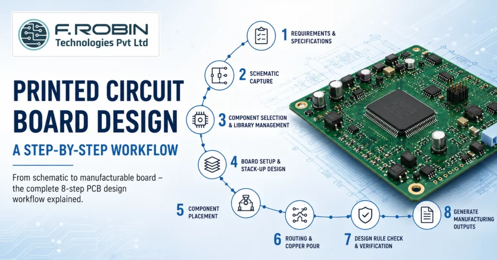
Printed circuit board design is the structured process of turning a circuit idea into a manufacturable board that powers almost every electronic product you use. Whether you are building a simple sensor module or a complex multi-layer system, the workflow follows the same logical path. Moreover, getting that path right the first time saves weeks of rework and thousands in respin costs. In this guide, we break down the complete printed circuit board design workflow into eight clear stages. You will learn what happens at each step, why it matters, and how to avoid the mistakes that trip up even experienced engineers. By the end, you will understand exactly how a schematic becomes a finished board ready for the factory. What Is Printed Circuit Board Design? Printed circuit board design is the process of creating the electrical and physical layout of a PCB so it can be reliably manufactured and assembled. In short, it converts a schematic — a diagram of how components connect — into a precise set of copper traces, layers, and footprints on a board. The process spans two linked activities. First, schematic design defines the logical connections between components. Second, board layout design places those components and routes the copper that joints them. Together, these stages form the foundation of every working electronic product. A complete PCB design also includes the manufacturing data the factory needs, such as Gerber files, drill files, and a bill of materials. Consequently, good design is about far more than drawing traces — it is about producing a board that works, lasts, and can actually be built at scale. Why the Printed Circuit Board Design Workflow Matters Following a disciplined workflow is the single biggest factor in first-pass success. Because each stage feeds the next, a small error early on multiplies downstream. For example, a wrong footprint chosen during component selection can force a complete respin after fabrication. A structured PCB design process delivers clear benefits: In high-speed and mixed-signal products, the stakes rise further. Therefore, many teams pair their layout work with signal integrity analysis to verify performance before the board is ever built. The 8-Step Printed Circuit Board Design Workflow Here is the end-to-end printed circuit board design workflow, stage by stage. Each step builds on the last, so resist the urge to skip ahead. Step 1: Define Requirements and Specifications Start with a clear specification. Capture the board’s function, operating voltages, signal speeds, environmental conditions, size limits, and target cost. Additionally, note any standards the board must meet, such as IPC Class 2 or Class 3. A solid spec becomes the reference you check every later decision against. Step 2: Schematic Capture Next, draw the schematic. During schematic capture, you place component symbols and wire their connections to define the netlist — the master list of every electrical connection. Use clear net names, add design notes, and run an electrical rule check (ERC) to catch missing connections or conflicting outputs early. Step 3: Component Selection and Library Management Now choose real parts for every symbol. Verify availability, footprint accuracy, and electrical ratings. Crucially, use trusted library data — a wrong land pattern is one of the most common causes of unassemblable boards. Strong library management keeps footprints, symbols, and 3D models consistent across projects. Step 4: Board Setup and Stack-Up Design Define the physical board: outline, layer count, and stack-up. The stack-up sets how signal, power, and ground layers are arranged, along with dielectric thicknesses. For high-speed nets, this is where you plan controlled impedance. As a rule, every signal layer should have an adjacent reference plane for a clean return path. Layer Count Typical Use 2 Layers Simple, low-speed, cost-sensitive boards 4 Layers Most products; dedicated power and ground planes 6–8 Layers High-speed digital, dense routing, controlled impedance 10+ Layers Complex multi-processor and HDI designs Step 5: Component Placement With the board set up, position your parts. Good placement drives everything that follows. Group related circuits, keep high-speed paths short, separate analog from digital, and place connectors and mounting holes per the mechanical drawing. Smart placement makes routing easier and improves thermal and signal performance at the same time. Step 6: Routing and Copper Pour Now connect the dots. Routing lays the copper traces that carry each signal, while a copper pour fills open areas — usually with ground — to improve return paths, shielding, and heat spreading. Match trace widths to current, control impedance on critical nets, and avoid sharp acute angles. Route power and high-speed signals first, then fill in the rest. Step 7: Design Rule Check and Verification Before release, run a design rule check (DRC). The DRC flags violations such as traces too close together, undersized clearances, or unconnected nets. Fix every error, then verify against your original spec. For demanding boards, add pre/post-layout simulation to confirm signal and power integrity. Step 8: Generate Manufacturing Outputs Finally, export the data the factory needs: Gerber (RS-274X) or ODB++ files, an NC drill file, a bill of materials, and assembly drawings. Review these outputs carefully, because they are what actually gets built. A clean handoff here connects your design directly to PCB manufacturing and assembly. PCB Design Tools Compared Your toolset shapes how efficiently you move through the PCB design workflow. The table below compares three widely used options. Tool Best For Notes Altium Designer Professional, high-speed, and complex multi-layer boards Unified environment with strong routing and library management OrCAD (Cadence) Enterprise teams needing advanced simulation Tight integration with Cadence analysis tools KiCad Startups, makers, and budget-conscious teams Free and open-source with a fast-growing feature set There is no single “best” tool — the right choice depends on board complexity, budget, and team workflow. Many engineers learn on KiCad and graduate to OrCAD or Altium Designer for high-speed production work. Best Practices for Printed Circuit Board Design Apply these proven practices to raise quality on every project: For products with tight enclosures, coordinate early with mechanical integration so the board fits and cools correctly.
How to Choose a PCB Design Company (12-Point Checklist)

Choosing the right PCB design company can make or break your hardware project. The right partner ships clean, manufacturable boards on time; the wrong one drains your budget with respins, missed deadlines, and IP worries. So before you sign anything, you need a way to separate a capable PCB design company from a risky one. This 12-point checklist gives you exactly that. We cover technical capability, trust and IP protection, process and communication, and commercial and local fit. Whether you are searching for a “pcb design company near me,” evaluating a PCB design firm in Chennai, or comparing offshore PCB design services, these 12 questions will help you commit with confidence. Why Choosing the Right PCB Design Company Matters Your PCB design company shapes the cost, reliability, and time-to-market of your entire product. Because layout errors surface only after fabrication, a weak partner can cost you weeks and lakhs in respins. A strong one, by contrast, catches problems early and hands you a board that simply works. The stakes are highest for complex boards. High-speed, mixed-signal, and dense designs demand real expertise, not just software access. Therefore, vetting your PCB design services partner carefully is not bureaucracy it is risk management. The checklist below turns that vetting into a simple, repeatable process. Consider the ripple effects too. A delayed board pushes back firmware, testing, certification, and launch, so a single weak link in design can slip an entire product roadmap. Conversely, a partner who gets the layout right the first time protects every downstream milestone. That is why the few hours you spend vetting a partner up front pay back many times over. The 12-Point Checklist for Choosing a PCB Design Company Work through these four areas. Each contains three questions to ask any candidate before you commit. Technical Capability (Points 1–3) Trust, IP & Confidentiality (Points 4–6) Process & Communication (Points 7–9) Commercial & Local Fit (Points 10–12) Quick Checklist Table Use this summary to score any candidate at a glance. Check What “Good” Looks Like 1. Domain Experience Similar boards successfully designed in your industry 2. Complexity Capability Experience with high-speed, multilayer, and mixed-signal designs 3. Tools & Standards Professional design tools and IPC compliance 4. NDA Offered Signed without hesitation to protect intellectual property 5. In-House Design No hidden subcontracting or outsourcing 6. Data & Ownership You retain ownership of all design files and deliverables 7. DFM Review Design for Manufacturability review completed before release 8. Communication Single point of contact with clear project updates and cadence 9. Deliverable Package Complete manufacturing data package provided 10. Transparent Pricing No hidden fees or unexpected charges 11. Local Fit Convenient collaboration and time-zone alignment 12. Ability to Scale Support from prototype development through volume production In-House vs Outsourced PCB Design Company Should you build a layout team or hire a PCB design company? The table below compares the options. Factor In-House Team PCB Design Company Upfront Cost High (salaries, software licenses, and hardware) Low (project-based engagement) Flexibility Fixed capacity based on team size Scales up or down with project demand Expertise Range Limited to the skills of your hired engineers Broad experience across industries and project types Tool Licensing You purchase and maintain design tools Typically included as part of the service Best For Continuous, high-volume PCB development Variable workloads or specialized design requirements For most teams with variable workloads, a capable PCB design firm delivers senior expertise without the fixed overhead. Many companies blend both keeping core work in-house and outsourcing specialized or overflow projects to trusted PCB design services. Red Flags to Watch For Beyond the checklist, these warning signs should give you pause: If you spot several of these, keep looking. The cost of choosing the wrong partner always exceeds the cost of vetting carefully. How to Run Your Evaluation (Step by Step) Turn the checklist into action with a simple process: This structured approach removes guesswork. Moreover, a paid pilot is the single most reliable predictor of how a partner will perform on your full project. Local vs Offshore: Weighing a Partner Near You Location affects collaboration, cost, and IP comfort. A nearby firm say, one in Chennai or elsewhere in India offers shared working hours, easier face-to-face reviews, and quicker design iterations. Offshore options may look cheaper, yet timezone gaps and slower feedback can erode that saving on complex boards. For many Indian OEMs and startups, a Make in India PCB service strikes the best balance: local collaboration, strong IP protection, and the option to keep design and manufacturing under one roof. Weigh proximity against capability and never trade away expertise purely to be close. If you searched for a “pcb design company near me,” use distance as a tie-breaker between strong candidates, not as the deciding factor on its own. Key Takeaways Conclusion Choosing a PCB design company does not have to be a gamble. Run every candidate through the 12-point checklist technical capability, trust and IP protection, process and communication, and commercial and local fit and the right partner becomes obvious. Above all, insist on a clear NDA, genuine in-house design, a DFM review, and transparent pricing. Looking for a Reliable PCB Design Partner? If you want a partner that ticks all 12 boxes, our PCB layout design services combine in-house engineering expertise, IPC-compliant quality, and a Make in India PCB service that supports your project from prototype through volume production. Discuss your requirements with our engineering team and move your next board forward with confidence. Talk to Our Engineering Team Frequently Asked Questions 1. How do I choose a PCB design company? Evaluate a candidate across four areas: technical capability, trust and IP protection, process and communication, and commercial and local fit. Use a 12-point checklist and require a signed NDA, DFM review, and a full deliverable package. 2. What should I ask a PCB design company before hiring? Ask about domain experience, complexity capability, tools and standards, NDA and IP handling, in-house design, DFM review, communication cadence, deliverables, pricing
HDI PCB Design Guide: The Ultimate Expert Resource (2026)
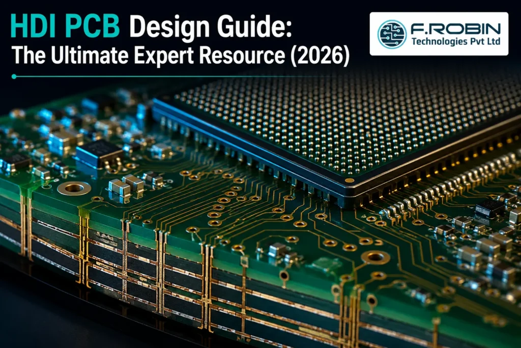
HDI PCB design guide — this is the resource electronics engineers, hardware architects, and product teams need when a conventional multilayer board can no longer meet the density, performance, or size requirements of a modern design. High-Density Interconnect (HDI) technology delivers routing density 4–8 times higher than standard multilayer PCBs. It enables the fine-pitch BGA escape routing, compact form factors, and high-speed signal performance that today’s smartphones, 5G modules, automotive radar systems, medical wearables, and aerospace avionics demand. But HDI introduces a substantially more complex set of design rules, manufacturing constraints, and cost tradeoffs that standard PCB design guidelines do not address. This ultimate guide covers everything: what HDI is and when you need it, how to choose the right stackup structure, microvia design rules, BGA escape routing strategies, signal integrity for HDI layouts, DFM requirements, manufacturing process overview, cost structure, and how to choose the right fabrication partner. Every section is backed by current IPC standards and factory-proven engineering data. What Is HDI PCB? Definition and Standards (what-is-hdi-pcb) HDI PCB (High-Density Interconnect Printed Circuit Board) is a category of printed circuit board defined by finer trace geometries, smaller via structures, and higher interconnect density per unit area than conventional multilayer PCBs. Per IPC-2226 — the governing international standard for HDI PCB design — an HDI board is characterised by: Quick Definition — What Is an HDI PCB? An HDI PCB (High-Density Interconnect Printed Circuit Board) is a printed circuit board that uses laser-drilled microvias (typically <150 μm diameter), fine traces (≤100 μm), and sequential lamination to achieve significantly higher wiring density and shorter signal paths than standard multilayer PCBs. Governed by IPC-2226, HDI technology enables fine-pitch BGA routing, compact electronic form factors, and improved electrical performance for advanced products such as smartphones, automotive radar systems, 5G modules, aerospace electronics, and medical devices. The HDI standard also defines a classification system — Type I through Type VI — based on the number and arrangement of microvia layers, which is covered in detail in the stackup section below. HDI PCB vs. Standard Multilayer PCB — Key Differences (hdi-vs-standard-multilayer) All HDI PCBs are multilayer, but not all multilayer PCBs are HDI. The key distinction is via technology and feature size. HDI PCB vs. Standard Multilayer PCB — Key Differences Parameter Standard Multilayer PCB HDI PCB Via type Mechanically drilled through-hole Laser-drilled microvias, blind, buried Minimum via diameter >200 μm (8 mil) 50–150 μm Minimum trace/space 100–150 μm (4–6 mil) 50–100 μm (2–4 mil) Pad density <20 pads/cm² >20 pads/cm² Routing density vs. standard Baseline 4–8× higher Layer construction Single lamination Sequential lamination cycles BGA pitch support 0.8 mm and above 0.4 mm and below Cost premium Baseline 1.3–6× depending on complexity Manufacturing complexity Standard High — multiple build-up cycles The fundamental advantage of HDI is the elimination of through-hole vias, which pass through every layer regardless of whether a connection is needed on that layer. This wastes routing space on every layer the via passes through. Microvias connect only the layers that actually need the connection, freeing up routing channels throughout the board. When Does Your Design Need HDI? (when-does-your-design-need-hdi) HDI is not the right choice for every design. It adds manufacturing complexity and cost that is only justified when specific design requirements cannot be met with conventional multilayer PCB technology. Conditions that indicate HDI is needed When standard multilayer is sufficient Consider standard multilayer PCB design best practices before committing to HDI. If your minimum BGA pitch is 0.8 mm or larger, your trace/space requirements are 4 mil or wider, and your board size is not tightly constrained, a conventional multilayer board almost certainly meets your needs at lower cost and with shorter lead times. Decision Rule — When Should You Use HDI PCB? Consider HDI PCB technology when your design includes BGAs with pitch below 0.8 mm, requires via-in-pad routing for fine-pitch components, needs line/space below 100/100 μm (4/4 mil), or when conventional through-hole vias consume excessive routing area. The HDI cost premium — typically 1.3× to 3× higher than standard multilayer PCBs — is justified when HDI enables: Smaller board size and compact form factor Reduced total layer count Improved high-speed signal performance Manufacturability of ultra-dense BGA layouts Advanced routing impossible with conventional PCB technology HDI Stackup Types — 1+N+1, 2+N+2, ELIC, and More (hdi-stackup-types) HDI stackup notation uses the formula i + N + i, where: 1+N+1 — Standard HDI (Type I/II) Structure: 1 build-up layer on each side of N core layers Typical layer count: 4–6 total layers Build-up dielectric thickness: ~30 μm per build-up layer Microvia capability: Blind vias from outer layers to first inner layer only Cost premium over standard PCB: +30–50% Best for: Medium-density designs, BGAs with 0.5–0.8 mm pitch, designs transitioning from conventional multilayer A 1+N+1 HDI stackup is the most common entry point into HDI. It adds one laser-drilled build-up layer to each side of a conventional core, enabling blind via escape routing from BGA pads on the outer layers without through-hole vias consuming routing space on inner layers. 2+N+2 — Advanced HDI (Type III) Structure: 2 build-up layers on each side of N core layers Typical layer count: 6–10 total layers Microvia capability: Two-tier microvias — stacked or staggered — enabling connections from outer layer to deeper inner layers Cost premium: +80–150% over standard PCB; 40–50% less than ELIC Yield: 85–90% production yield (vs. 70–75% for ELIC) Reliability: Passes 2,000 thermal cycles per IPC-TM-650 2.6.7 with less than 5% resistance change in microvias Best for: Advanced mobile devices, automotive radar, 5G RF modules, aerospace avionics with BGAs at 0.4–0.5 mm pitch The 2+N+2 structure is the sweet spot for most high-performance HDI designs. It balances routing density, manufacturing yield, and cost more effectively than ELIC while supporting the fine-pitch BGAs and high-speed interfaces that advanced products require. An 8-layer 2+4+2 HDI board replaces a 12-layer conventional board for equivalent routing density, reducing material cost by approximately 25%. ELIC (Every Layer Interconnect) — Any-Layer HDI Structure: No rigid core — all
How Power Integrity Analysis Prevents Costly PCB Failures

Power integrity analysis is the step most PCB design teams skip — until a board fails in the field and no one can explain why. The symptoms are familiar: random resets, corrupted data, thermal hotspots, intermittent logic errors. Nine times out of ten, the root cause isn’t the schematic. It’s the power delivery network quietly failing to deliver clean, stable voltage to the components that depend on it. Modern ICs operate on rails as low as 0.8 V with tolerances tighter than ±3%. A 30 mV voltage drop that would have been irrelevant on legacy 5 V hardware is now the difference between a functioning system and a field return. PI analysis finds these problems during layout — when fixing them costs engineering hours, not full board respins. This guide covers what power integrity analysis is, what it catches, and how it protects your PCB’s reliability from design through production. What Is Power Integrity Analysis? Power integrity analysis is the simulation-based process of validating that every component on a PCB receives clean, stable voltage within its specified tolerance — under all operating conditions. It evaluates three distinct but related phenomena: PI analysis uses EDA tools — Ansys SIwave, Cadence PowerDC, Siemens HyperLynx PI — to model your actual PCB geometry, stackup, via structures, and decoupling capacitor placement. The result is a quantitative prediction of your power delivery performance before a single board is manufactured. Definition Power integrity analysis is the simulation-driven validation of a PCB’s power distribution network to prevent voltage drop, resonance, and noise from causing functional or reliability failures. Why PCB Power Integrity Failures Are Hard to Diagnose Power integrity failures are particularly damaging because they mimic other failure modes. An engineer chasing a firmware bug or a signal integrity issue may spend weeks before tracing the root cause to a collapsing power rail. Here’s why they’re difficult to catch without PI analysis: They’re load-dependent. A rail may measure correctly at idle but sag below minimum voltage under peak current load — the exact condition during functional testing or in-field operation. They’re frequency-dependent. PDN resonance only becomes destructive at specific switching frequencies. A board may pass bench validation at room temperature only to fail after thermal soak shifts component behavior. They’re intermittent. Voltage sag during a DDR memory burst or FPGA fabric switching event lasts nanoseconds. Standard bench probing misses it entirely without a high-bandwidth power rail probe and deliberate triggering. Running power integrity analysis during layout eliminates the guesswork. Instead of diagnosing failures on physical hardware, engineers identify and fix them in simulation — where the iteration cost is near zero. What PI Analysis Catches: The Four Critical Failure Modes 1. IR Drop — Voltage Starvation at the Load IR drop occurs when DC current flows through copper traces and planes with finite resistance. The voltage at the load is always lower than the source voltage, and in high-current designs that difference can be significant. A 2 A load drawing current through a narrow trace with 15 mΩ of resistance loses 30 mV — a 3.75% drop on a 0.8 V rail that immediately puts the IC outside its specified operating window. IR drop analysis produces color-coded voltage maps across your entire copper geometry, identifying exactly which paths exceed your voltage budget. 2. PDN Resonance — Noise Amplification at Specific Frequencies Every power distribution network has resonant frequencies governed by its inductance and capacitance. At resonance, PDN impedance spikes. Any switching energy injected at that frequency — from a voltage regulator, FPGA switching fabric, or DDR memory bus — gets amplified rather than absorbed. PDN resonance often explains why a design passes bench testing but fails EMI compliance. The noise is there; it’s just waiting for the right operating condition to become destructive. 3. Insufficient or Misplaced Decoupling — Capacitors That Don’t Contribute Decoupling capacitors suppress transient voltage drops by providing local charge. But their effectiveness depends on placement, value, and package size. A 100 nF capacitor placed 15 mm from an IC power pin has more inductance in its connection path than capacitance in its operating range. It contributes almost nothing to PDN impedance at the frequencies that matter. PI analysis shows which capacitors are actively reducing impedance and which are dead weight. This allows engineers to eliminate unnecessary components and reposition effective ones — reducing BOM cost while improving power integrity. 4. Voltage Ripple — Rail Noise That Corrupts Sensitive Circuits Voltage ripple is the AC noise riding on top of a nominally stable DC supply. Its sources include switching regulator output ripple (at the converter’s switching frequency and harmonics), simultaneous switching outputs (SSO) from high-density I/O banks, and load current transients during memory bursts or processor state changes. For most digital logic, moderate ripple is tolerable. For ADCs, PLLs, RF front ends, and high-speed SerDes interfaces, it is not. Even millivolt-level noise on a PLL supply rail introduces phase jitter. Millivolt noise on an ADC reference rail degrades SNR in ways that look like a firmware calibration problem until the power rail is measured with sufficient bandwidth. How IR Drop Analysis Works IR drop analysis is the DC simulation component of power integrity analysis. The workflow: A properly executed IR drop analysis catches the difference between a 0.9 V rail delivering 0.9 V at the source and 0.83 V at the IC power pin — a 7.7% deviation that guarantees intermittent failure under load. PDN Analysis and Target Impedance Explained PDN analysis extends power integrity into the frequency domain. The goal is to keep the PDN impedance below a calculated target value — the target impedance — across the full frequency range where your devices switch. Target impedance formula: Z_target = ΔV ÷ ΔI Where ΔV is your acceptable voltage ripple (typically 5% of rail voltage) and ΔI is the peak transient current demand. Worked example: A 1.0 V rail with a 5% ripple budget and a 2 A transient load → Z_target = 0.05 ÷ 2 = 25 mΩ PDN analysis plots
Multilayer PCB Design Best Practices: 10 Expert Tips (2026)
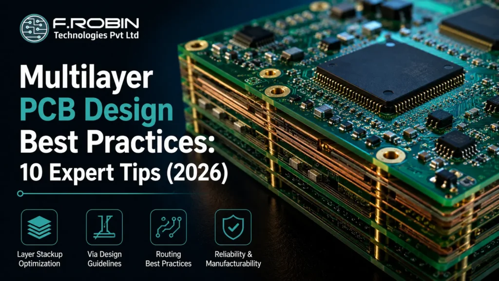
Multilayer PCB design best practices are what separate boards that pass EMC testing and work reliably in the field from those that don’t. As signals run faster, components shrink smaller, and certification requirements grow stricter, getting the fundamentals right before layout begins has never been more critical. This guide walks you through 10 proven best practices — from stackup planning and impedance control to thermal management and DFM so your multilayer design gets it right before a single Gerber file is sent to fabrication. What Is Multilayer PCB Design? Multilayer PCB design is the process of creating printed circuit boards with three or more copper layers separated by dielectric (insulating) materials, laminated under heat and pressure into a single rigid structure. Each layer serves a dedicated purpose signal routing, power distribution, or ground reference — enabling engineers to pack far more functionality into a smaller board footprint than single- or double-layer designs allow. Multilayer PCBs are the foundation of virtually every high-performance electronic product today: smartphones, industrial controllers, medical imaging equipment, 5G base stations, automotive ECUs, and aerospace avionics all rely on them. Quick Definition Multilayer PCB design involves boards with 3 or more copper layers — common counts are 4, 6, 8, 10, 12, and 16+ — that provide dedicated planes for power delivery, signal return paths, controlled impedance routing, and higher component density for complex electronic designs. When Does a Design Need More Than Two Layers? Not every board needs to be multilayer. However, your design almost certainly does if it includes any of the following: If any of these apply, the question is no longer whether to go multilayer it’s how many layers and how to structure them. That’s exactly what the following best practices cover. Best Practice 1 — Plan Your Layer Stackup First The stackup is the architectural blueprint of your multilayer PCB. It defines the number of layers, their sequence, the dielectric material between them, and the copper thickness on each layer. Plan your stackup before routing a single trace. Every impedance calculation, every signal layer assignment, and every power plane decision flows from it. Changing the stackup mid-layout invalidates every impedance-controlled trace and forces expensive re-routing. Key Stackup Principles Standard Stackup Reference Layer Count Typical Arrangement Best For 4-layer Signal / GND / PWR / Signal Medium-density microcontrollers, IoT, industrial 6-layer Signal / GND / Signal / Signal / PWR / Signal RF segregation, additional routing space 8-layer Signal / GND / Signal / GND / PWR / Signal / GND / Signal DDR, PCIe, multi-power-rail SoC designs 12+ layer Complex alternating signal/plane Advanced FPGA, telecom, aerospace Best Practice 2 — Choose the Right Layer Count More layers are not always better. Each additional layer adds fabrication cost, increases board thickness, and complicates via drilling and lamination. Too few layers, however, force routing compromises that degrade performance and EMC behaviour. Best Practice 3 — Master Signal Integrity and Impedance Control Signal integrity (SI) is the discipline of ensuring signals propagate accurately without distortion, ringing, or reflections. In multilayer PCB design, SI is controlled primarily through impedance management. What Is Controlled Impedance? Controlled impedance means designing trace geometry width and thickness — alongside dielectric thickness so that the characteristic impedance of a trace matches the system impedance. Typical targets: How to Achieve Controlled Impedance Best Practice 4 — Use Solid Ground Planes and Manage Return Paths The ground plane is not just a reference potential it is an active participant in signal transmission. Return current travels in the ground plane directly beneath a signal trace, following the path of least inductance, not least resistance. Ground Plane Best Practices Per the IPC- 2221 generic requirement of the design, maintaining continuous ground reference planes is a fundamental requirement for reliable high-speed multilayer PCB designs. Best Practice 5 — Route High-Speed Signals on Inner Layers Inner signal layers use a stripline geometry — the trace is sandwiched between two reference planes, which confine the electric field to the dielectric and provide natural EMI shielding on both sides. When to Use Inner vs. Outer Layers Signal Type Recommended Layer Reason Clock, DDR, PCIe, high-speed bus Inner (stripline) Shielded between reference planes; lower EMI Low-speed I/O, LED control, power signals Outer (microstrip) Easy access; EMI not critical RF / antenna traces Outer with controlled reference distance Specific impedance and radiation requirements Differential pairs (USB, HDMI, Ethernet) Inner preferred, outer acceptable Keep pairs on same layer; minimise layer changes Keep differential pairs on the same layer throughout their entire route. Every layer change via is an impedance discontinuity. If a layer change is unavoidable, use matched-length via stubs and place the transition well away from connectors and receivers. Best Practice 6 — Control Crosstalk With Layer Routing Direction Crosstalk is unwanted signal coupling between adjacent traces. In multilayer PCBs, the risk is highest between parallel traces on adjacent signal layers. The Perpendicular Routing Rule Route adjacent signal layers perpendicular to each other: This perpendicular relationship minimises the length over which traces on adjacent layers run parallel, dramatically reducing both capacitive and inductive coupling between them. Additional Crosstalk Reduction Techniques Best Practice 7 — Choose and Place Vias Strategically Vias are the vertical interconnects between layers. Via selection and placement directly affect routing density, signal quality, and manufacturing cost. Via Types in Multilayer PCBs Via Type Description Best Use Through-hole via Drilled through all layers Standard inter-layer connections; lowest cost Blind via Connects outer layer to one or more inner layers only BGA escape routing; saves routing space on unused layers Buried via Connects two inner layers only; not visible from outside Ultra-high-density designs; higher fabrication cost Microvia (laser-drilled) ≤0.15 mm diameter; HDI boards only Fine-pitch BGA (0.5 mm pitch and below) Engineering Insight Through-hole vias are the most economical option for standard multilayer PCBs, while blind, buried, and microvias are commonly used in HDI (High-Density Interconnect) designs to improve routing density and signal integrity for fine-pitch components. Via Placement Best Practices Best Practice 8 — Manage Thermal Distribution Across
EMI and EMC Explained for PCB & Electronics Design
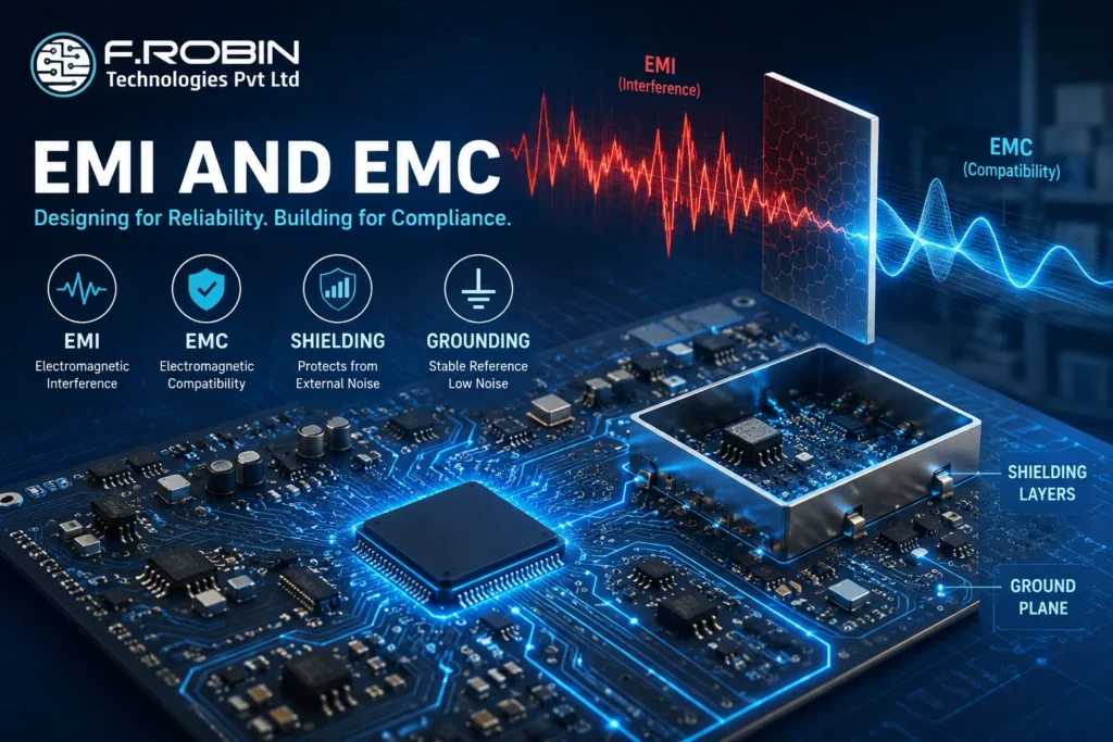
EMI and EMC are critical concepts in modern electronics, PCB engineering, and embedded system design. Electronic devices today operate in highly connected and signal-dense environments. From smartphones and industrial automation systems to automotive ECUs and medical electronics, every electronic product must function reliably without creating or receiving unwanted electromagnetic disturbances. This is where EMI and EMC become essential in electronics and PCB engineering. Electromagnetic interference (EMI) can disrupt signals, reduce device performance, and even cause system failures. Electromagnetic compatibility (EMC), on the other hand, ensures that electronic systems operate correctly without interfering with nearby devices. Understanding EMI and EMC is essential for PCB designers, embedded engineers, electronics manufacturers, and product development teams aiming to build reliable and standards-compliant products. In this guide, we will explain: What Is EMI? Electromagnetic Interference (EMI) refers to unwanted electromagnetic noise or signals that disrupt the normal operation of electronic devices. EMI can originate from: EMI affects signal integrity and may lead to: Common Examples of EMI What Is EMC? Electromagnetic Compatibility (EMC) is the ability of an electronic device to operate correctly in its electromagnetic environment without causing or experiencing interference. An EMC-compliant product: EMC is critical for: Difference Between EMI and EMC EMI vs EMC Comparison Table Parameter EMI EMC Full Form Electromagnetic Interference Electromagnetic Compatibility Meaning Unwanted electromagnetic noise Ability to function without interference Focus Problem source System immunity and compliance Impact Causes signal disruption Prevents malfunction Goal Reduce interference Ensure reliable operation Common Solution Shielding and filtering Compliance-focused PCB design Simple Explanation EMI is the interference itself, while EMC is the ability of a system to handle or avoid that interference. Types of EMI in Electronics 1. Conducted EMI Conducted EMI travels through electrical conductors such as: Sources 2. Radiated EMI Radiated EMI spreads through electromagnetic waves in the air. Sources Why EMI and EMC Matter in PCB Design EMI in PCB Design Poor PCB layout is one of the leading causes of electromagnetic interference. Common PCB EMI Problems PCB Design Areas That Affect EMC High-speed PCB designs require strong EMC considerations to avoid compliance failures. Best PCB Design Practices for EMC 1. Use Proper Ground Planes Continuous ground planes reduce return path impedance and lower EMI emissions. 2. Minimize Loop Areas Smaller current loops reduce electromagnetic radiation. 3. Separate Analog and Digital Signals This prevents noise coupling between sensitive circuits. 4. Add Decoupling Capacitors Decoupling capacitors stabilize power integrity and reduce switching noise. 5. Optimize Layer Stack-Up A proper multilayer PCB structure improves EMC performance significantly. For advanced PCB layout optimization, explore the professional PCB design solutions offered by Frobintech PCB Layout Design Services . EMI and EMC Testing Explained What Is EMI and EMC Testing? EMI and EMC testing verifies whether an electronic product: Main EMC Tests Test Type Purpose Radiated Emissions Measures electromagnetic radiation Conducted Emissions Measures noise through conductors ESD Testing Evaluates electrostatic discharge immunity Surge Testing Checks power surge resistance RF Immunity Testing Measures resistance to RF interference Why EMC Testing Is Important EMC testing helps manufacturers prevent product failures, meet certification requirements, improve product reliability, reduce field issues, and achieve faster market approval. EMC Compliance and Industry Standards Products must satisfy regulatory electromagnetic standards before entering the market. Proper EMC compliance helps ensure reliable device operation, reduces interference risks, and supports global certification requirements. Important EMC Standards Products failing EMC compliance may: EMI Shielding Techniques EMI shielding reduces electromagnetic noise using conductive or magnetic materials. Common EMI Shielding Methods Metal Shielding Uses aluminum or copper enclosures to block electromagnetic waves. Shielded Cables Protect signal integrity in noisy environments. Ferrite Beads Suppress high-frequency noise in circuits. Ground Shielding Improves electromagnetic containment in PCB layouts. EMI Filters Reduce conducted interference in power lines. Best Practices to Reduce EMI and Improve EMC Practical EMC Design Guidelines Use Shorter Signal Traces Shorter traces reduce antenna effects and radiation. Maintain Proper Grounding Good grounding lowers noise coupling. Avoid Sharp Trace Angles Use 45-degree bends to improve signal flow. Use Differential Pair Routing Improves noise immunity in high-speed circuits. Apply EMI Shielding Shield sensitive areas from RF interference. Perform Pre-Compliance Testing Early testing helps identify EMC problems before production. Key Takeaways Conclusion As electronic systems become faster and more compact, understanding EMI and EMC is increasingly important for engineers and manufacturers. From PCB design and embedded systems to industrial automation and consumer electronics, electromagnetic compatibility directly affects product reliability, compliance, and performance. By implementing proper grounding, shielding, filtering, and PCB layout techniques, companies can reduce electromagnetic interference and improve EMC compliance effectively. Organizations developing advanced electronic products should prioritize EMI and EMC considerations early in the design cycle to avoid costly redesigns and certification failures. Need Expert PCB Layout Support? Need expert support for EMC-friendly PCB layouts and high-speed electronics design? Explore professional PCB design solutions from Frobintech PCB Layout Design Services For project discussions and engineering consultation, contact the team here: Contact Frobintech FAQ
Why Signal Integrity Analysis Is Critical in High-Speed PCB Design

Signal integrity analysis is the difference between hardware that works on the first spin and hardware stuck in a six-week debug loop. As data rates push into multi-gigabit territory, every trace, via, and connector on your PCB becomes a potential failure point — and the physics will not wait for you to find it on the bench. Whether you are designing DDR5 memory interfaces, PCIe Gen 4/5 links, USB 3.x, or high-speed LVDS connections, signal integrity in PCB design is not an optional step. It is the engineering discipline that determines whether your board ships on schedule or gets pulled back for a costly respin. What Is Signal Integrity Analysis? Signal integrity (SI) analysis is the process of evaluating how electrical signals behave as they travel through PCB interconnects — traces, vias, connectors, and IC packages. The goal is straightforward: ensure that signals arrive at their destination accurately, without distortion, timing errors, or noise corruption. At its core, PCB signal integrity analysis examines three domains: Here is the physics reality that makes this non-optional: any PCB trace longer than roughly one-sixth of the signal’s wavelength behaves as a transmission line, not a simple wire. At 1 GHz, a quarter-wavelength in FR-4 is approximately 30 mm. Most high-speed nets are longer than that — which means transmission line effects on PCB are always present in modern high-speed designs. Why Signal Integrity Matters in High-Speed PCB Design The physics does not negotiate. When rise times fall below 1 nanosecond — standard in FPGAs, DDR5, PCIe Gen 4/5, and USB 3.x — signal integrity in PCB design directly determines whether a board functions or fails in production. Hardware Respins Are Expensive A PCB respin caused by signal integrity problems typically costs 4 to 12 weeks and tens of thousands of dollars in engineering time, board fabrication, and component procurement. Catching the same problem at the design stage is a zero-cost layout edit. Pre-layout SI analysis is among the highest-ROI activities in hardware development. EMC Compliance Depends on It Radiated emissions from high-speed PCB traces that are improperly routed, referenced, or terminated cause products to fail FCC, CE, and CISPR 32 compliance testing. Fixing electromagnetic interference in PCB design during layout costs nothing. Failing an EMC test after production can delay a product launch by months. Data Rates Leave Zero Margin At 10 Gbps, one unit interval is 100 picoseconds. Jitter, crosstalk, and reflections consume that margin fast. PCB noise reduction through deliberate design is the only reliable way to maintain acceptable bit error rates in serial interfaces like PCIe, SATA, and high-speed LVDS. The Five Most Common SI Failure Modes Understanding the failure modes is the first step in preventing them. 1. Reflections When a signal encounters an impedance discontinuity — at a via, connector, or unterminated stub — part of it reflects back toward the source. PCB reflection analysis reveals this as overshoot, undershoot, and ringing on the waveform. Impedance-controlled PCB design eliminates most reflection problems by maintaining consistent trace impedance end-to-end. 2. Crosstalk PCB crosstalk analysis quantifies the electromagnetic coupling between adjacent traces. Near-end crosstalk (NEXT) and far-end crosstalk (FEXT) inject noise onto quiet nets, causing false triggers in digital logic and SNR degradation in analog signals. Maintaining the 3W rule — spacing traces at least three times the trace width apart — and using differential pair routing are the primary countermeasures. 3. Ground Bounce When multiple output drivers switch simultaneously, parasitic inductance in the power and ground paths creates voltage spikes on the reference rails. Ground bounce shifts logic switching thresholds unpredictably and is often misdiagnosed as a signal problem when it is actually a power delivery failure. 4. Skin Effect and Dielectric Loss At high frequencies, current concentrates on the outer surface of a conductor, increasing effective trace resistance. Combined with dielectric loss in the PCB substrate, this causes high-frequency signal components to attenuate faster than low-frequency ones — limiting usable bandwidth on long traces in high-frequency PCB design. 5. Differential Pair Skew PCB trace length matching is critical for differential protocols. If the two traces in a pair have different physical lengths, a timing skew develops that degrades common-mode noise rejection. For interfaces above 1 Gbps, most design rules require length matching within 5 mils. 4. Signal Integrity vs. Power Integrity Power integrity and signal integrity address different failure modes but interact directly. A clean signal riding on a noisy power rail degrades unpredictably. Always run both analyses together. Aspect Signal Integrity (SI) Power Integrity (PI) Focus Waveform quality across interconnects Stable power delivery to IC pins Primary Concern Reflections, crosstalk, jitter, skew Voltage droop, rail noise, PDN impedance Key Parameters Trace impedance, rise time, termination Bypass capacitance, VRM response Tools TDR, eye diagram, IBIS simulation VNA, PDN simulation, power planes Interaction Rail noise degrades switching thresholds SI switching creates power transients Best Practice: A design with perfect impedance control can still fail if the power delivery network introduces voltage transients that shift logic switching thresholds. SI and PI must always be co-analysed. PCB Parameters That Directly Affect Signal Integrity Trace Impedance and PCB Stackup Design Characteristic impedance depends on trace width, dielectric height, and material Dk. Impedance-controlled PCB design targets 50 Ω single-ended and 100 Ω differential — specified on fabrication drawings and verified by the PCB manufacturer using TDR coupons. Deviations above ±10% produce measurable reflections at high data rates. Via Stubs A via that passes through multiple layers but connects at only a few creates a dangling stub. Stubs act as resonant elements that cause signal attenuation at specific frequencies. Back-drilling or using blind/buried vias eliminates stubs for designs operating above 5 Gbps. Reference Plane Continuity Every high-speed trace needs a continuous, unbroken reference plane beneath it. Routing over plane splits, cutouts, or large antipads increases trace inductance, disrupts return current paths, and creates electromagnetic interference hotspots in PCB designs. Termination Strategy PCB impedance matching through proper termination absorbs signal energy to prevent reflections. Source termination places a series resistor at the driver; parallel
