
Signal integrity analysis is the difference between hardware that works on the first spin and hardware stuck in a six-week debug loop. As data rates push into multi-gigabit territory, every trace, via, and connector on your PCB becomes a potential failure point — and the physics will not wait for you to find it on the bench.
Whether you are designing DDR5 memory interfaces, PCIe Gen 4/5 links, USB 3.x, or high-speed LVDS connections, signal integrity in PCB design is not an optional step. It is the engineering discipline that determines whether your board ships on schedule or gets pulled back for a costly respin.
What Is Signal Integrity Analysis?
Signal integrity (SI) analysis is the process of evaluating how electrical signals behave as they travel through PCB interconnects — traces, vias, connectors, and IC packages. The goal is straightforward: ensure that signals arrive at their destination accurately, without distortion, timing errors, or noise corruption.
At its core, PCB signal integrity analysis examines three domains:
- Timing integrity — signals meet setup and hold time requirements at receiver ICs
- Voltage-level integrity — logic levels remain within valid switching thresholds
- Noise immunity — interference does not cause false triggering or data errors
Here is the physics reality that makes this non-optional: any PCB trace longer than roughly one-sixth of the signal’s wavelength behaves as a transmission line, not a simple wire. At 1 GHz, a quarter-wavelength in FR-4 is approximately 30 mm. Most high-speed nets are longer than that — which means transmission line effects on PCB are always present in modern high-speed designs.
Why Signal Integrity Matters in High-Speed PCB Design
The physics does not negotiate. When rise times fall below 1 nanosecond — standard in FPGAs, DDR5, PCIe Gen 4/5, and USB 3.x — signal integrity in PCB design directly determines whether a board functions or fails in production.
Hardware Respins Are Expensive
A PCB respin caused by signal integrity problems typically costs 4 to 12 weeks and tens of thousands of dollars in engineering time, board fabrication, and component procurement. Catching the same problem at the design stage is a zero-cost layout edit. Pre-layout SI analysis is among the highest-ROI activities in hardware development.
EMC Compliance Depends on It
Radiated emissions from high-speed PCB traces that are improperly routed, referenced, or terminated cause products to fail FCC, CE, and CISPR 32 compliance testing. Fixing electromagnetic interference in PCB design during layout costs nothing. Failing an EMC test after production can delay a product launch by months.
Data Rates Leave Zero Margin
At 10 Gbps, one unit interval is 100 picoseconds. Jitter, crosstalk, and reflections consume that margin fast. PCB noise reduction through deliberate design is the only reliable way to maintain acceptable bit error rates in serial interfaces like PCIe, SATA, and high-speed LVDS.
The Five Most Common SI Failure Modes
Understanding the failure modes is the first step in preventing them.
1. Reflections
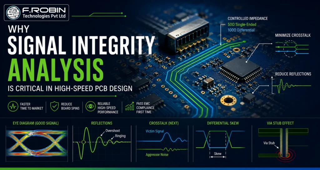
When a signal encounters an impedance discontinuity — at a via, connector, or unterminated stub — part of it reflects back toward the source. PCB reflection analysis reveals this as overshoot, undershoot, and ringing on the waveform. Impedance-controlled PCB design eliminates most reflection problems by maintaining consistent trace impedance end-to-end.
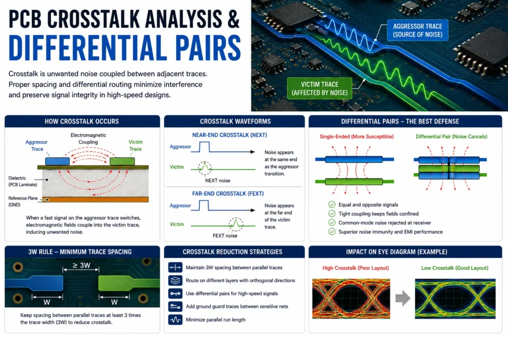
2. Crosstalk
PCB crosstalk analysis quantifies the electromagnetic coupling between adjacent traces. Near-end crosstalk (NEXT) and far-end crosstalk (FEXT) inject noise onto quiet nets, causing false triggers in digital logic and SNR degradation in analog signals. Maintaining the 3W rule — spacing traces at least three times the trace width apart — and using differential pair routing are the primary countermeasures.
3. Ground Bounce
When multiple output drivers switch simultaneously, parasitic inductance in the power and ground paths creates voltage spikes on the reference rails. Ground bounce shifts logic switching thresholds unpredictably and is often misdiagnosed as a signal problem when it is actually a power delivery failure.
4. Skin Effect and Dielectric Loss
At high frequencies, current concentrates on the outer surface of a conductor, increasing effective trace resistance. Combined with dielectric loss in the PCB substrate, this causes high-frequency signal components to attenuate faster than low-frequency ones — limiting usable bandwidth on long traces in high-frequency PCB design.
5. Differential Pair Skew
PCB trace length matching is critical for differential protocols. If the two traces in a pair have different physical lengths, a timing skew develops that degrades common-mode noise rejection. For interfaces above 1 Gbps, most design rules require length matching within 5 mils.
4. Signal Integrity vs. Power Integrity
Power integrity and signal integrity address different failure modes but interact directly. A clean signal riding on a noisy power rail degrades unpredictably. Always run both analyses together.
| Aspect | Signal Integrity (SI) | Power Integrity (PI) |
|---|---|---|
| Focus | Waveform quality across interconnects | Stable power delivery to IC pins |
| Primary Concern | Reflections, crosstalk, jitter, skew | Voltage droop, rail noise, PDN impedance |
| Key Parameters | Trace impedance, rise time, termination | Bypass capacitance, VRM response |
| Tools | TDR, eye diagram, IBIS simulation | VNA, PDN simulation, power planes |
| Interaction | Rail noise degrades switching thresholds | SI switching creates power transients |
PCB Parameters That Directly Affect Signal Integrity
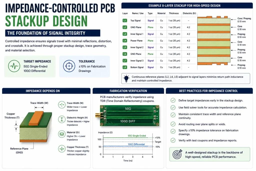
Trace Impedance and PCB Stackup Design
Characteristic impedance depends on trace width, dielectric height, and material Dk. Impedance-controlled PCB design targets 50 Ω single-ended and 100 Ω differential — specified on fabrication drawings and verified by the PCB manufacturer using TDR coupons. Deviations above ±10% produce measurable reflections at high data rates.
Via Stubs
A via that passes through multiple layers but connects at only a few creates a dangling stub. Stubs act as resonant elements that cause signal attenuation at specific frequencies. Back-drilling or using blind/buried vias eliminates stubs for designs operating above 5 Gbps.
Reference Plane Continuity
Every high-speed trace needs a continuous, unbroken reference plane beneath it. Routing over plane splits, cutouts, or large antipads increases trace inductance, disrupts return current paths, and creates electromagnetic interference hotspots in PCB designs.
Termination Strategy
PCB impedance matching through proper termination absorbs signal energy to prevent reflections. Source termination places a series resistor at the driver; parallel termination places one at the receiver. Choosing the wrong strategy for a given topology is one of the most common causes of eye diagram failures in SI simulation.
How SI Simulation Works in Practice
Signal integrity simulation uses electrical models of PCB interconnects and IC I/O buffers to predict waveform behaviour before any hardware is built. The standard six-step workflow:
- Extract geometry
trace widths, layer stackup, and via structures become transmission line models
- Import IBIS models
captures non-linear drive and receive characteristics without proprietary SPICE models
- Define scenarios
single-bit responses, worst-case data patterns, and statistical eye diagrams
- Run simulation
SPICE-based or EM field solvers propagate signals through the model
- Analyse results
eye diagrams, time-domain waveforms, and S-parameters reveal where the design fails its margins
- Iterate
adjust trace widths, spacing, and termination until all interfaces meet specification
Common SI simulation tools include Cadence Sigrity, Mentor HyperLynx, Ansys SIwave, and Keysight ADS. Pre-layout SI analysis — simulating before routing begins — is the most cost-effective mode because it establishes routing constraints before any physical work is done.
Best Practices for High-Speed PCB Layout
These PCB routing best practices align with IPC-2141B, IPC-2152, and high-speed interface design guidelines.
Impedance Control
- Define target impedances in the stackup before layout begins
- Specify ±10% tolerance on fabrication drawings
- Use field solvers — not rule-of-thumb calculators — for traces above 5 Gbps
Differential Pair Routing
- Route pairs together with consistent spacing throughout their entire length
- Match trace lengths within 5 mils for links above 1 Gbps
- Avoid routing differential pairs across plane splits or through via-dense regions
Via Management
- Minimise via counts — each via adds 0.5 to 1.5 nH of parasitic inductance
- Back-drill vias for data rates above 5 Gbps to remove resonant stubs
- Add return-path vias adjacent to signal vias when transitioning between reference planes
Crosstalk Mitigation
- Maintain 3W spacing for parallel high-speed nets
- Route parallel high-speed traces on different layers with orthogonal routing directions where possible
- Use guard traces between sensitive analog and noisy digital signal groups
8.With vs. Without SI Analysis — The Real Cost Difference
| Factor | Without SI Analysis | With SI Analysis |
|---|---|---|
| Average Board Spins | 2–4 | 1–1.5 |
| EMC First-Pass Rate | ~40% | >80% |
| Impedance Control | Ad hoc, often incorrect | Defined, validated, documented |
| Crosstalk Detection | Found on the bench | Predicted and fixed in layout |
| Via Stub Impact | Ignored until failure | Evaluated and back-drilled if needed |
| Design Confidence | Low — requires extensive debug | High — margins quantified before fab |
| Time to Market | Delayed by debug cycles | Accelerated through predictive design |
Key Takeaways
- Signal integrity analysis predicts and prevents waveform degradation before hardware is built
- The primary SI failure modes are reflections, crosstalk, ground bounce, and differential pair skew
- Impedance-controlled PCB design and correct termination are the most effective structural fixes
- SI simulation using IBIS models quantifies design margins without needing physical hardware
- Power integrity and signal integrity must always be analysed together
- Pre-layout SI analysis is the most cost-effective point in the design cycle to catch and fix problems
Conclusion
Signal integrity problems are predictable — and entirely preventable. Running SI analysis early, designing for impedance control, and following disciplined routing practices are what separate first-pass hardware from costly board respins. If your design carries any high-speed interface, signal integrity analysis is not the last item on the checklist. It is the first.
Need Reliable High-Speed PCB Design?
Frobin Tech delivers impedance-controlled PCB layouts with signal integrity built in from day one.
Frequently Asked Questions
Signal integrity analysis evaluates how electrical signals behave through PCB interconnects examining reflections, crosstalk, timing, and noise. It is essential for any design with clock frequencies above 100 MHz or data rates above 500 Mbps.
Reflections occur at impedance discontinuities — wherever trace impedance changes abruptly, such as at a via, connector, or unterminated stub. Impedance-controlled design and proper termination eliminate the majority of reflection problems.
A PCB fabricated so that specific signal traces achieve a defined characteristic impedance — typically 50 Ω single-ended or 100 Ω differential — controlled through trace width, dielectric thickness, and PCB material selection in the stackup.
The stackup determines dielectric height, material properties, and layer arrangement — all of which directly control trace impedance. A well-designed stackup places continuous reference planes adjacent to high-speed signal layers, minimising return path inductance and supporting required impedance targets.
Pre-layout SI simulation is most effective — it sets routing constraints before physical work begins. Post-layout simulation then verifies the routed design meets those constraints. Running simulation only after layout is complete significantly reduces its value.
Signal integrity focuses on waveform quality across interconnects. Power integrity focuses on stable power delivery to IC pins. Both must be analysed together — power rail noise directly degrades signal noise margins.
