
Printed circuit board design is the structured process of turning a circuit idea into a manufacturable board that powers almost every electronic product you use. Whether you are building a simple sensor module or a complex multi-layer system, the workflow follows the same logical path. Moreover, getting that path right the first time saves weeks of rework and thousands in respin costs.
In this guide, we break down the complete printed circuit board design workflow into eight clear stages. You will learn what happens at each step, why it matters, and how to avoid the mistakes that trip up even experienced engineers. By the end, you will understand exactly how a schematic becomes a finished board ready for the factory.
What Is Printed Circuit Board Design?
Printed circuit board design is the process of creating the electrical and physical layout of a PCB so it can be reliably manufactured and assembled. In short, it converts a schematic — a diagram of how components connect — into a precise set of copper traces, layers, and footprints on a board.
The process spans two linked activities. First, schematic design defines the logical connections between components. Second, board layout design places those components and routes the copper that joints them. Together, these stages form the foundation of every working electronic product.
A complete PCB design also includes the manufacturing data the factory needs, such as Gerber files, drill files, and a bill of materials. Consequently, good design is about far more than drawing traces — it is about producing a board that works, lasts, and can actually be built at scale.
Why the Printed Circuit Board Design Workflow Matters
Following a disciplined workflow is the single biggest factor in first-pass success. Because each stage feeds the next, a small error early on multiplies downstream. For example, a wrong footprint chosen during component selection can force a complete respin after fabrication.
A structured PCB design process delivers clear benefits:
- Fewer respins. Catching issues in simulation costs pennies; catching them after fabrication costs weeks.
- Lower manufacturing cost. Designing for manufacturability keeps yields high and rejects low.
- Better reliability. Proper stack-up, grounding, and routing reduce noise, heat, and field failures.
- Faster time-to-market. A repeatable flow lets teams move quickly without cutting corners.
In high-speed and mixed-signal products, the stakes rise further. Therefore, many teams pair their layout work with signal integrity analysis to verify performance before the board is ever built.
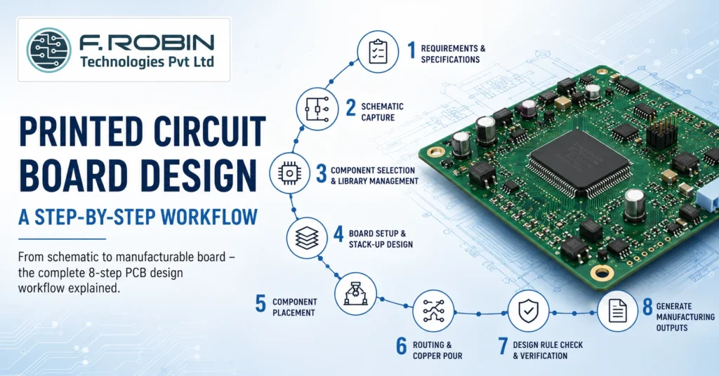
The 8-Step Printed Circuit Board Design Workflow
Here is the end-to-end printed circuit board design workflow, stage by stage. Each step builds on the last, so resist the urge to skip ahead.
Step 1: Define Requirements and Specifications
Start with a clear specification. Capture the board’s function, operating voltages, signal speeds, environmental conditions, size limits, and target cost. Additionally, note any standards the board must meet, such as IPC Class 2 or Class 3. A solid spec becomes the reference you check every later decision against.
Step 2: Schematic Capture
Next, draw the schematic. During schematic capture, you place component symbols and wire their connections to define the netlist — the master list of every electrical connection. Use clear net names, add design notes, and run an electrical rule check (ERC) to catch missing connections or conflicting outputs early.
Step 3: Component Selection and Library Management
Now choose real parts for every symbol. Verify availability, footprint accuracy, and electrical ratings. Crucially, use trusted library data — a wrong land pattern is one of the most common causes of unassemblable boards. Strong library management keeps footprints, symbols, and 3D models consistent across projects.
Step 4: Board Setup and Stack-Up Design
Define the physical board: outline, layer count, and stack-up. The stack-up sets how signal, power, and ground layers are arranged, along with dielectric thicknesses. For high-speed nets, this is where you plan controlled impedance. As a rule, every signal layer should have an adjacent reference plane for a clean return path.
| Layer Count | Typical Use |
|---|---|
| 2 Layers | Simple, low-speed, cost-sensitive boards |
| 4 Layers | Most products; dedicated power and ground planes |
| 6–8 Layers | High-speed digital, dense routing, controlled impedance |
| 10+ Layers | Complex multi-processor and HDI designs |
Step 5: Component Placement
With the board set up, position your parts. Good placement drives everything that follows. Group related circuits, keep high-speed paths short, separate analog from digital, and place connectors and mounting holes per the mechanical drawing. Smart placement makes routing easier and improves thermal and signal performance at the same time.
Step 6: Routing and Copper Pour
Now connect the dots. Routing lays the copper traces that carry each signal, while a copper pour fills open areas — usually with ground — to improve return paths, shielding, and heat spreading. Match trace widths to current, control impedance on critical nets, and avoid sharp acute angles. Route power and high-speed signals first, then fill in the rest.
Step 7: Design Rule Check and Verification
Before release, run a design rule check (DRC). The DRC flags violations such as traces too close together, undersized clearances, or unconnected nets. Fix every error, then verify against your original spec. For demanding boards, add pre/post-layout simulation to confirm signal and power integrity.
Step 8: Generate Manufacturing Outputs
Finally, export the data the factory needs: Gerber (RS-274X) or ODB++ files, an NC drill file, a bill of materials, and assembly drawings. Review these outputs carefully, because they are what actually gets built. A clean handoff here connects your design directly to PCB manufacturing and assembly.
PCB Design Tools Compared
Your toolset shapes how efficiently you move through the PCB design workflow. The table below compares three widely used options.
| Tool | Best For | Notes |
|---|---|---|
| Altium Designer | Professional, high-speed, and complex multi-layer boards | Unified environment with strong routing and library management |
| OrCAD (Cadence) | Enterprise teams needing advanced simulation | Tight integration with Cadence analysis tools |
| KiCad | Startups, makers, and budget-conscious teams | Free and open-source with a fast-growing feature set |
There is no single “best” tool — the right choice depends on board complexity, budget, and team workflow. Many engineers learn on KiCad and graduate to OrCAD or Altium Designer for high-speed production work.
Best Practices for Printed Circuit Board Design
Apply these proven practices to raise quality on every project:
- Design for manufacturability (DFM) from the start. Respect your fab’s minimum trace, space, and drill rules.
- Keep return paths continuous. Never route a high-speed signal across a plane split.
- Plan the stack-up early. Layer arrangement affects impedance, noise, and cost.
- Use length matching for buses like DDR and differential pairs such as USB and PCIe.
- Add test points so the board can be tested and debugged after assembly.
- Document everything. Clear assembly notes and a complete data pack prevent factory questions and delays.
For products with tight enclosures, coordinate early with mechanical integration so the board fits and cools correctly.
Common Printed Circuit Board Design Mistakes to Avoid
Even seasoned designers fall into these traps. Watch for them:
- Wrong footprints. Always verify land patterns against the datasheet and IPC standards.
- Ignoring the stack-up. A poor stack-up causes impedance and EMI problems that are hard to fix later.
- Routing before placement is final. Rework explodes when placement keeps changing.
- Skipping the DRC. Releasing with unresolved violations almost guarantees a respin.
- Forgetting decoupling capacitors. Inadequate decoupling leads to noise and random resets.
- No design-for-test features. Boards without test points are expensive to troubleshoot in volume.
Avoiding these errors is often the difference between a one-pass success and three costly board spins.
Key Takeaways
- Printed circuit board design converts a schematic into a manufacturable, reliable board.
- The workflow has eight stages, from requirements to manufacturing outputs.
- Schematic capture, placement, routing, copper pour, and stack-up are the core technical steps.
- A design rule check and clean manufacturing data are essential before release.
- Tools like Altium Designer, OrCAD, and KiCad each suit different needs and budgets.
- Following DFM and verifying early dramatically cuts respins and cost.
Conclusion
Printed circuit board design follows a clear, repeatable path: define the spec, capture the schematic, choose components, set the stack-up, place parts, route the copper, verify with a DRC, and release clean manufacturing data. When you respect each stage, you build boards that work the first time, cost less to manufacture, and reach the market faster.
Need Expert PCB Layout Design Support?
If you would rather hand the process to specialists, our PCB layout design services cover everything from schematic capture to manufacturing-ready output. Discuss your project requirements with our engineering team and accelerate your next board design with confidence.
Contact UsFrequently Asked Questions
1. What is a multilayer PCB?
A multilayer PCB is a circuit board with three or more conductive copper layers bonded together with insulating material, combining signal layers with power and ground planes.
2. How many layers does a multilayer PCB need?
Most products use 4 layers. Simple boards may use 2, while high-speed, dense, or multi-processor board designs often require 6, 8, or more layers.
3. Why use a multilayer PCB instead of a 2-layer board?
A multilayer PCB offers cleaner power delivery, better signal integrity, lower EMI, and higher routing density thanks to dedicated power and ground planes.
4. What is a PCB layer stack?
A layer stack, or stack-up, is the vertical arrangement of signal layers and power/ground planes. It determines impedance, return paths, and manufacturability.
5. Is a 4-layer PCB always better than a 2-layer PCB?
Not always. A 4-layer board performs better for high-speed or dense designs, but a 2-layer board is more cost-effective and perfectly suitable for simple, low-speed circuits.
