
HDI PCB design guide — this is the resource electronics engineers, hardware architects, and product teams need when a conventional multilayer board can no longer meet the density, performance, or size requirements of a modern design.
High-Density Interconnect (HDI) technology delivers routing density 4–8 times higher than standard multilayer PCBs. It enables the fine-pitch BGA escape routing, compact form factors, and high-speed signal performance that today’s smartphones, 5G modules, automotive radar systems, medical wearables, and aerospace avionics demand. But HDI introduces a substantially more complex set of design rules, manufacturing constraints, and cost tradeoffs that standard PCB design guidelines do not address.
This ultimate guide covers everything: what HDI is and when you need it, how to choose the right stackup structure, microvia design rules, BGA escape routing strategies, signal integrity for HDI layouts, DFM requirements, manufacturing process overview, cost structure, and how to choose the right fabrication partner. Every section is backed by current IPC standards and factory-proven engineering data.
What Is HDI PCB? Definition and Standards (what-is-hdi-pcb)
HDI PCB (High-Density Interconnect Printed Circuit Board) is a category of printed circuit board defined by finer trace geometries, smaller via structures, and higher interconnect density per unit area than conventional multilayer PCBs.
Per IPC-2226 — the governing international standard for HDI PCB design — an HDI board is characterised by:
- Microvias of less than 150 μm diameter (typically 50–100 μm for laser-drilled)
- Trace width and spacing of 100 μm (approximately 4 mil) or finer
- Pad density exceeding 20 pads per cm²
- Use of blind and/or buried vias in addition to or instead of through-hole vias
- Sequential lamination — multiple lamination cycles to build up layers incrementally
Quick Definition — What Is an HDI PCB?
An HDI PCB (High-Density Interconnect Printed Circuit Board) is a printed circuit board that uses laser-drilled microvias (typically <150 μm diameter), fine traces (≤100 μm), and sequential lamination to achieve significantly higher wiring density and shorter signal paths than standard multilayer PCBs.
Governed by IPC-2226, HDI technology enables fine-pitch BGA routing, compact electronic form factors, and improved electrical performance for advanced products such as smartphones, automotive radar systems, 5G modules, aerospace electronics, and medical devices.
The HDI standard also defines a classification system — Type I through Type VI — based on the number and arrangement of microvia layers, which is covered in detail in the stackup section below.
HDI PCB vs. Standard Multilayer PCB — Key Differences (hdi-vs-standard-multilayer)
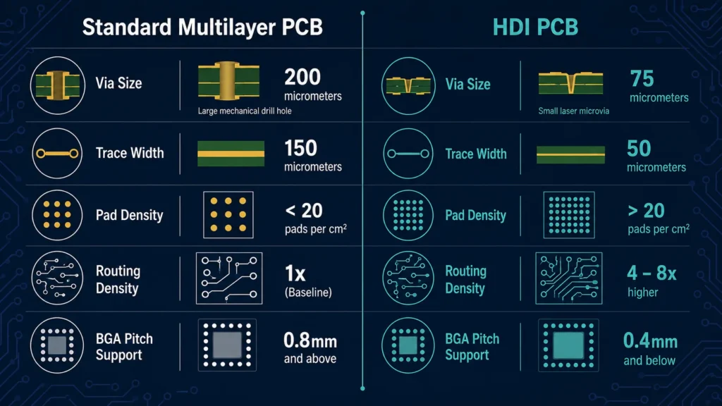
All HDI PCBs are multilayer, but not all multilayer PCBs are HDI. The key distinction is via technology and feature size.
HDI PCB vs. Standard Multilayer PCB — Key Differences
| Parameter | Standard Multilayer PCB | HDI PCB |
|---|---|---|
| Via type | Mechanically drilled through-hole | Laser-drilled microvias, blind, buried |
| Minimum via diameter | >200 μm (8 mil) | 50–150 μm |
| Minimum trace/space | 100–150 μm (4–6 mil) | 50–100 μm (2–4 mil) |
| Pad density | <20 pads/cm² | >20 pads/cm² |
| Routing density vs. standard | Baseline | 4–8× higher |
| Layer construction | Single lamination | Sequential lamination cycles |
| BGA pitch support | 0.8 mm and above | 0.4 mm and below |
| Cost premium | Baseline | 1.3–6× depending on complexity |
| Manufacturing complexity | Standard | High — multiple build-up cycles |
The fundamental advantage of HDI is the elimination of through-hole vias, which pass through every layer regardless of whether a connection is needed on that layer. This wastes routing space on every layer the via passes through. Microvias connect only the layers that actually need the connection, freeing up routing channels throughout the board.
When Does Your Design Need HDI? (when-does-your-design-need-hdi)
HDI is not the right choice for every design. It adds manufacturing complexity and cost that is only justified when specific design requirements cannot be met with conventional multilayer PCB technology.
Conditions that indicate HDI is needed
- Fine-pitch BGAs below 0.8 mm pitch — standard dog-bone via escape routing cannot physically fit in the available pad pitch at 0.5 mm and below; microvias and via-in-pad are required
- Board size constraints — the design requires a physically smaller board than conventional routing can accommodate
- Layer count reduction — HDI can replace an 8–10 layer conventional board with a 4–6 layer HDI board, reducing both thickness and cost when correctly applied
- High-speed signal performance — shorter interconnect paths in HDI reduce parasitic capacitance and inductance, improving signal integrity at GHz frequencies
- High component density — the design has more components per unit area than standard routing can accommodate without HDI
- Mixed signal isolation — HDI’s tight reference planes and short via stubs support better isolation between analog and digital domains
When standard multilayer is sufficient
Consider standard multilayer PCB design best practices before committing to HDI. If your minimum BGA pitch is 0.8 mm or larger, your trace/space requirements are 4 mil or wider, and your board size is not tightly constrained, a conventional multilayer board almost certainly meets your needs at lower cost and with shorter lead times.
Decision Rule — When Should You Use HDI PCB?
Consider HDI PCB technology when your design includes BGAs with pitch below 0.8 mm, requires via-in-pad routing for fine-pitch components, needs line/space below 100/100 μm (4/4 mil), or when conventional through-hole vias consume excessive routing area.
The HDI cost premium — typically 1.3× to 3× higher than standard multilayer PCBs — is justified when HDI enables:
- Smaller board size and compact form factor
- Reduced total layer count
- Improved high-speed signal performance
- Manufacturability of ultra-dense BGA layouts
- Advanced routing impossible with conventional PCB technology
HDI Stackup Types — 1+N+1, 2+N+2, ELIC, and More (hdi-stackup-types)
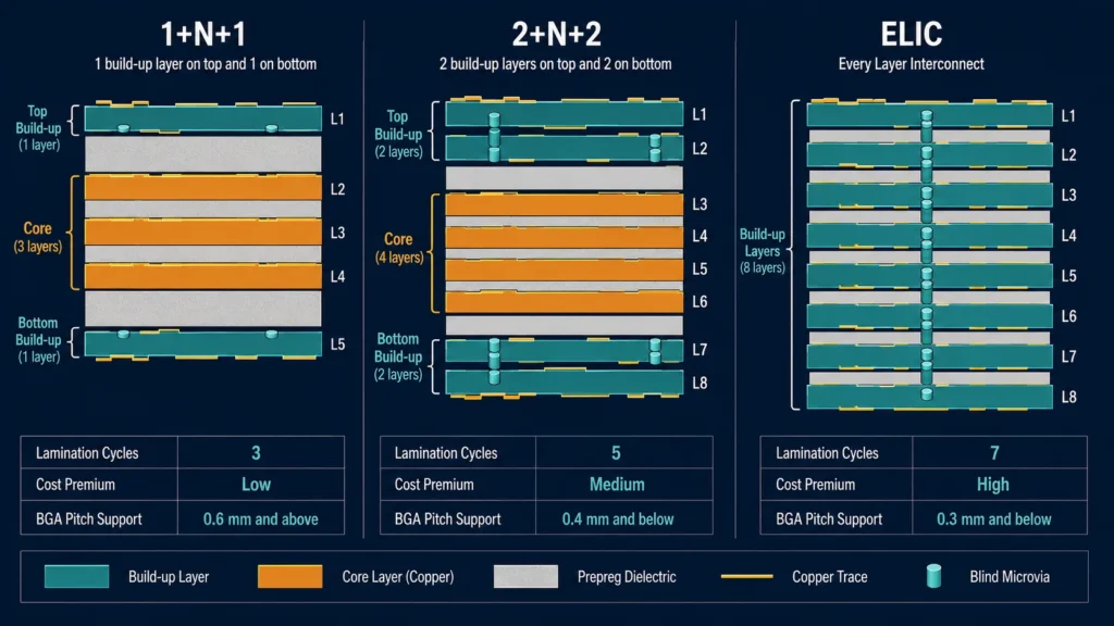
HDI stackup notation uses the formula i + N + i, where:
- i = number of build-up layers on each side of the core
- N = number of core layers in the centre of the stackup
- Each build-up layer adds one tier of microvia connectivity and one lamination cycle
1+N+1 — Standard HDI (Type I/II)
Structure: 1 build-up layer on each side of N core layers
Typical layer count: 4–6 total layers
Build-up dielectric thickness: ~30 μm per build-up layer
Microvia capability: Blind vias from outer layers to first inner layer only
Cost premium over standard PCB: +30–50%
Best for: Medium-density designs, BGAs with 0.5–0.8 mm pitch, designs transitioning from conventional multilayer
A 1+N+1 HDI stackup is the most common entry point into HDI. It adds one laser-drilled build-up layer to each side of a conventional core, enabling blind via escape routing from BGA pads on the outer layers without through-hole vias consuming routing space on inner layers.
2+N+2 — Advanced HDI (Type III)
Structure: 2 build-up layers on each side of N core layers
Typical layer count: 6–10 total layers
Microvia capability: Two-tier microvias — stacked or staggered — enabling connections from outer layer to deeper inner layers
Cost premium: +80–150% over standard PCB; 40–50% less than ELIC
Yield: 85–90% production yield (vs. 70–75% for ELIC)
Reliability: Passes 2,000 thermal cycles per IPC-TM-650 2.6.7 with less than 5% resistance change in microvias
Best for: Advanced mobile devices, automotive radar, 5G RF modules, aerospace avionics with BGAs at 0.4–0.5 mm pitch
The 2+N+2 structure is the sweet spot for most high-performance HDI designs. It balances routing density, manufacturing yield, and cost more effectively than ELIC while supporting the fine-pitch BGAs and high-speed interfaces that advanced products require.
An 8-layer 2+4+2 HDI board replaces a 12-layer conventional board for equivalent routing density, reducing material cost by approximately 25%.
ELIC (Every Layer Interconnect) — Any-Layer HDI
Structure: No rigid core — all layers are build-up layers interconnected by stacked microvias on every layer
Typical layer count: 8–14 layers
Microvia capability: Full any-layer connectivity — a microvia can connect any two adjacent layers at any location
Dielectric thickness: 12–20 μm ultra-thin
BGA pitch support: Down to 0.2 mm
Cost premium: 4–6× over standard PCB
Best for: Smartphone application processors, ultra-compact wearables, advanced military and aerospace electronics requiring maximum routing density
ELIC is the most technically demanding and expensive HDI structure. It requires up to 7 sequential lamination cycles and is typically only justified for the highest-density applications where 2+N+2 routing capacity is genuinely exhausted.
Coreless HDI
A variant of ELIC without a rigid core — used primarily in flexible-rigid hybrid designs and ultra-thin portable electronics. Layer count is typically 4–8 layers with 25 μm dielectric thickness.
HDI Stackup Selection Guide
| Requirement | Recommended Stackup |
|---|---|
| BGA pitch 0.65–0.8 mm, moderate density | Standard multilayer (no HDI needed) |
| BGA pitch 0.5 mm, medium density | 1+N+1 |
| BGA pitch 0.4 mm, high density, 5G/automotive | 2+N+2 |
| BGA pitch 0.3 mm, maximum density, mobile SoC | ELIC (Every Layer Interconnect) |
| Flexible or ultra-thin form factor | Coreless HDI |
Microvia Design Rules and Specifications (microvia-design-rules)
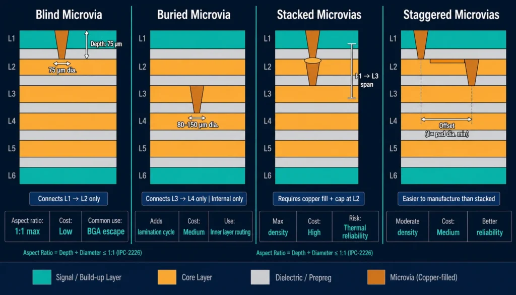
Microvias are the backbone of HDI PCB design. Getting their geometry and placement right determines board reliability, manufacturing yield, and long-term performance.
Microvia Types in HDI PCB Design
Blind microvias
Connect an outer layer to one inner layer only. The most common microvia type in HDI. Formed by laser drilling from the outer copper layer to the first inner layer, then copper-plated. Diameter typically 50–150 μm.
Buried microvias
Connect two inner layers only — not visible from either outer surface. Formed before final lamination. Adds a lamination cycle and cost but frees outer-layer routing space.
Stacked microvias
Multiple microvias aligned directly on top of each other, spanning more than one build-up layer (for example, Layer 1 → Layer 2 → Layer 3 in a 2+N+2 stackup). More compact than staggered but requires more robust plating, careful copper filling, and additional inspection. Higher risk of reliability failure at the stack joint under thermal cycling.
Staggered microvias
Microvias on adjacent build-up layers that are offset from each other rather than directly aligned. Easier and cheaper to manufacture than stacked; provides better thermal cycling reliability. Uses slightly more routing space than stacked.
Critical Microvia Parameters per IPC-2226 and IPC-6016
| Parameter | Standard Value | Notes |
|---|---|---|
| Maximum aspect ratio | 1:1 (depth:diameter) | 0.75:1 preferred for optimal plating quality |
| Typical microvia diameter | 75–100 μm | Confirm with your specific fabricator |
| Minimum pad diameter (capture pad) | Via diameter + 100–150 μm | Annular ring sufficient for drill registration |
| Minimum pad diameter (target pad) | Via diameter + 150–200 μm | Larger target pad for reliable connection |
| Copper fill requirement | Filled and capped for stacked vias | Prevents reliability failure at stack joint |
| Laser drill type | CO₂ (for copper/dielectric) or UV YAG (for copper-to-copper) | CO₂ most common for standard build-up |
Per IPC-2226, microvia aspect ratios of 1:1 are the maximum, with 0.75:1 preferred for optimal plating quality. For a 75 μm dielectric, this means a minimum hole diameter of 75 μm at 1:1, or 100 μm at 0.75:1. Higher aspect ratios create plating voids and reliability failures. Always confirm your fabricator’s specific capability before finalising microvia dimensions — some achieve 1:1 reliably; others prefer 0.6:1 or better.
Stacked vs. staggered microvia — decision guide
Use stacked microvias when:
- Maximum routing density is required and board space is critically constrained
- The design uses ELIC or 2+N+2 with dense BGA at 0.3–0.4 mm pitch
- The fabricator confirms capability for copper-filled, capped via stacks
Use staggered microvias when:
- Routing density allows for the lateral offset (typically one pad diameter or more)
- The design must pass stringent thermal cycling reliability requirements
- Manufacturing yield and cost are priorities over absolute routing density
BGA Escape Routing in HDI PCB Design (bga-escape-routing)
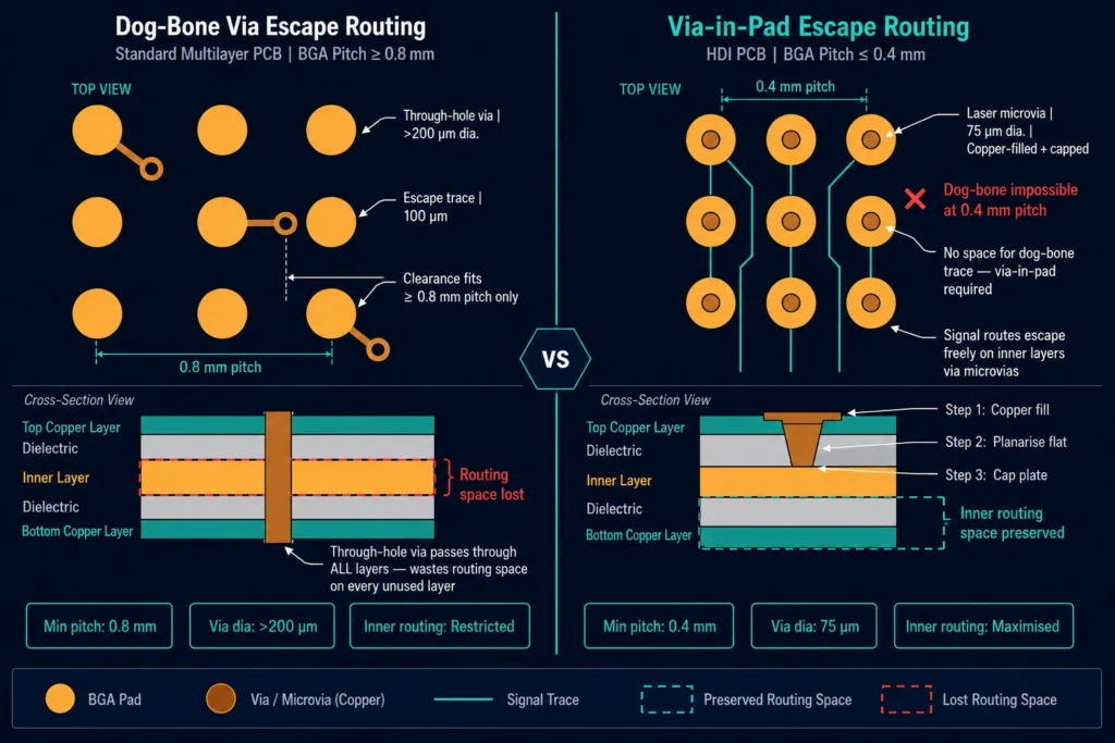
BGA escape routing is one of the primary drivers for choosing HDI over conventional multilayer technology. As BGA pitch shrinks below 0.8 mm, the physical space between pads becomes insufficient to route a trace between the BGA pads and out to a through-hole via using the conventional dog-bone pattern.
BGA Pitch vs. Escape Routing Strategy
| BGA Pitch | Escape Routing Strategy | Via Technology Required |
|---|---|---|
| 1.0 mm | Dog-bone — through-hole via outside pad | Standard multilayer |
| 0.8 mm | Dog-bone — tight but possible with 4 mil trace | Standard multilayer or 1+N+1 |
| 0.65 mm | Modified dog-bone or via-in-pad required | 1+N+1 HDI preferred |
| 0.5 mm | Via-in-pad required | 1+N+1 to 2+N+2 HDI |
| 0.4 mm | Via-in-pad, microvias only | 2+N+2 HDI |
| 0.3 mm | Via-in-pad, stacked microvias | ELIC |
Via-in-pad technique
Via-in-pad (VIP) places the microvia directly inside the BGA pad footprint rather than adjacent to it. This eliminates the need for the connecting trace between pad and via, freeing space for signal routing.
Via-in-pad requires mandatory processing steps:
- Copper filling — the via barrel must be completely filled with electroplated copper to prevent solder wicking into the via during reflow
- Planarisation — the filled via surface is mechanically planarised (lapped flat) to ensure a co-planar, solderable surface
- Cap plating — a thin copper cap is plated over the filled, planarised via to complete the pad surface
Skipping any of these steps results in solder joint voids, poor BGA collapse, or opens on assembled boards. Via-in-pad without proper fill and planarisation is one of the most common root causes of HDI assembly failures.
BGA escape routing best practices
- Route the outer ring of BGA balls on the same layer as the BGA, exiting the BGA footprint through the gaps between inner-row pads
- Use blind microvias from Layer 1 to Layer 2 (or Layer 2 to Layer 3 in 2+N+2) to route inner-ring BGA signals down to inner layers
- For very dense BGAs (0.4 mm pitch and below), every signal must escape through via-in-pad; there is no space for routing between pads on the surface layer
- Maintain consistent via fill and planarisation specifications across all via-in-pad features — do not mix filled and unfilled vias within the same BGA footprint
Signal Integrity in HDI PCB Design (signal-integrity-hdi)
HDI’s short interconnect paths and tight reference planes are natural advantages for signal integrity — but only when the design exploits them correctly. Several HDI-specific SI challenges require attention.
Advantages of HDI for signal integrity
- Shorter signal paths reduce parasitic capacitance and inductance. This directly improves rise time, reduces ringing, and enables higher data rates.
- Blind and buried vias eliminate via stubs. Through-hole vias on conventional multilayer boards create resonant stubs that degrade signals at specific frequencies. Microvias eliminate this problem entirely.
- Tighter reference plane spacing improves impedance control. The thin build-up dielectrics (30–50 μm) in HDI create very tightly coupled microstrip and stripline geometries, enabling accurate impedance control at fine trace widths.
HDI-specific signal integrity challenges
Microvia stub resonance Even in HDI, buried vias and incompletely drilled structures can create resonances. Verify all via structures against your signal frequencies. Stacked microvias spanning multiple build-up layers need SI simulation to confirm resonance-free performance at the target data rate.
Tight coupling and crosstalk Fine trace/space in HDI (50–75 μm) means adjacent traces couple more strongly. Apply the 3W rule — trace-to-trace spacing of at least 3× the trace width — for all critical signals. For differential pairs in ultra-HDI at 50 μm trace width, this means 150 μm minimum edge-to-edge spacing.
Impedance control in thin dielectrics Thin build-up dielectrics require very fine trace widths to achieve 50 Ω. At 30 μm dielectric thickness, a 50 Ω microstrip trace may be only 50–60 μm wide — at the edge of standard photolithography capability. Work with your fabricator to confirm achievable impedance tolerance (typically ±10% for HDI, ±8% for tighter requirements).
Power/ground plane resonance Thin dielectrics in HDI create very high inter-plane capacitance — beneficial for power integrity but can create resonance modes. Use electromagnetic simulation to identify resonance frequencies and place appropriate suppression components.
Keep solid reference planes under all high-speed traces. Use stitching vias near plane splits or edges to maintain ground continuity. For comprehensive signal integrity methodology, refer to our guide on signal integrity analysis.
Power Integrity and Decoupling in HDI Layouts (power-integrity-hdi)
Power delivery in HDI PCBs benefits from the inherently high inter-plane capacitance of thin dielectrics but requires careful decoupling strategy.
HDI power delivery best practices
- Use thin-dielectric power/ground plane pairs for embedded capacitance. A power-ground plane pair with 30 μm dielectric has approximately 3–5 nF/cm² of embedded capacitance — useful for high-frequency decoupling without discrete capacitors.
- Place decoupling capacitors on the same side as the IC. In HDI, the short microvia connecting a decoupling capacitor pad to the power plane is critical. Even a 50–75 μm microvia contributes inductance that limits effectiveness at frequencies above 1–2 GHz.
- Use a mix of capacitor values. A large bulk capacitor (10–100 μF) handles low-frequency demand; small ceramic capacitors (100 nF, 10 nF, 1 nF) handle progressively higher frequencies. In HDI with very fine pitch, 01005 package size capacitors are commonly required.
- Minimise the loop area between the IC power pin, decoupling capacitor, and the power plane. In HDI this means placing the capacitor pad as close to the BGA pad as the design rules allow, with the ground via immediately adjacent.
Thermal Management in HDI PCBs (thermal-management-hdi)
HDI’s high component density concentrates heat in smaller areas, making thermal management more not less critical than in conventional layouts.
HDI thermal management strategies
Thermal via arrays Arrays of copper-filled microvias beneath high-dissipation components (power regulators, RF amplifiers, processor packages) conduct heat from the component-facing surface down through the build-up layers to inner copper planes or heatsink structures.
- Use a regular grid of thermal vias within the component thermal pad footprint
- Specify copper fill for all thermal vias — unfilled vias have dramatically lower thermal conductivity
- Typical thermal via diameter: 100–150 μm with 250–300 μm pitch in the array
Copper plane coverage Maximise copper pour coverage on inner plane layers to distribute heat laterally. HDI’s thin dielectrics reduce the thermal resistance between copper layers, making inner planes more effective heat spreaders than in thick conventional stackups.
Component placement for thermal management
- Place high-dissipation components away from thermally sensitive devices (precision ADCs, oscillators, sensors)
- Cluster power components near board edges where heat can transfer to chassis or heat sink structures
- Verify via thermal resistance in simulation — even well-designed thermal via arrays have finite resistance that limits heat transfer
Material selection for high-temperature HDI For designs with significant power dissipation, consider build-up dielectrics with higher thermal conductivity than standard FR-4 derivatives. Low-loss materials like Rogers or Panasonic Megtron 6 offer improved thermal performance alongside their dielectric and signal integrity benefits.
Design for Manufacturability (DFM) for HDI (dfm-for-hdi)
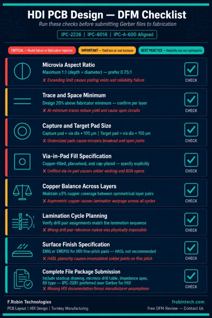
DFM for HDI is significantly more demanding than for conventional multilayer PCBs. HDI fabrication involves multiple lamination cycles, laser drilling, and sequential build-up processes — each with tight tolerances that must be reflected in the design.
Critical HDI DFM rules
Microvia specifications
- Confirm maximum aspect ratio with your specific fabricator before finalising microvia depth — do not assume the IPC maximum applies universally
- Specify microvia fill type clearly: copper-filled and capped for all stacked vias and all via-in-pad features
- Use consistent microvia diameters across the design — mixing diameters requires multiple laser drill setups and increases cost
Trace and space
- Design to 20% above your fabricator’s minimum capability for yield reliability
- For 2+N+2 and ELIC, confirm minimum trace/space on each build-up layer separately — capability often differs between outer build-up layers and inner core layers
- Allow for photolithographic resolution limits: at 50 μm trace/space, standard subtractive etching becomes unreliable; confirm whether mSAP (Modified Semi-Additive Process) is required
Pad sizes
- Capture pad diameter = microvia diameter + minimum 100 μm annular ring
- Target pad diameter = microvia diameter + minimum 150–200 μm
- Never reduce pad sizes to recover routing space — undersized pads are the leading cause of microvia reliability failures
Copper balance across layers
- HDI’s thin dielectrics and sequential lamination make copper balance even more critical than in conventional boards
- Unbalanced copper causes warping during lamination cycles that is difficult to correct
- Maintain within ±5% copper coverage balance across symmetrically placed layers
Lamination cycle planning
- Each build-up layer requires one lamination cycle; stacked microvias require their lower vias to be drilled, filled, and capped before the next build-up layer is laminated
- Verify your microvia depth references the correct layer pair for each lamination cycle — a common mistake is specifying a microvia from Layer 1 to Layer 3 in a 1+N+1 stackup, which is physically impossible and requires a 2+N+2 process
Solder mask and surface finish
- LDI (Laser Direct Imaging) is standard for HDI solder mask — confirm with your fabricator
- ENIG and ENEPIG are the preferred surface finishes for HDI fine-pitch BGA pads due to their flat, reliable soldering surface
- HASL is not recommended for HDI due to planarity issues with fine-pitch pads
Submitting HDI files — what to include
Beyond standard Gerber and BOM packages, HDI designs require:
- Detailed stackup drawing with all dielectric thicknesses, copper weights, and build-up layer sequence
- Microvia drill table specifying drill pair (from layer to layer), diameter, fill type, and cap requirement for each microvia class
- Impedance specification referencing each controlled-impedance layer by number with target impedance and tolerance
- Via fill specification — explicitly state filled/capped requirement; do not rely on defaults
- IPC-2581 format preferred over Gerber for HDI — it carries stackup and drill data in a single file that reduces ambiguity
HDI PCB Manufacturing Process — Step by Step (hdi-manufacturing-process)
Understanding the HDI manufacturing sequence helps designers make better DFM decisions and communicate more effectively with fabricators.
HDI Manufacturing Sequence for 1+N+1
Step-by-step HDI PCB fabrication workflow covering sequential lamination, laser drilling, microvia plating, planarisation, and final testing.
Core Fabrication
Inner core layers are fabricated using the standard multilayer PCB process, including inner layer imaging, oxide treatment, lamination, and mechanical drilling.
Core Electrical Testing
Flying probe or bed-of-nails testing validates the electrical integrity of the core before HDI build-up processing begins.
Build-Up Dielectric Lamination
Thin build-up dielectric material such as prepreg or resin-coated copper is laminated onto the PCB core.
Laser Drilling
CO₂ or UV laser systems drill microvias through the build-up dielectric to the target copper pads on the core layers.
Desmear Process
Plasma or chemical desmear removes laser-ablated residue from microvia walls to ensure reliable copper adhesion and plating quality.
Electroless Copper Deposition
A thin electroless copper seed layer is deposited on via walls to prepare the structure for electrolytic copper plating.
Electrolytic Copper Plating
Copper plating thickens the via barrel walls. For filled microvias, plating continues until the via cavity is completely filled with copper.
Via Planarisation
Filled vias are mechanically planarised to create a flat co-planar surface for reliable via-in-pad assembly.
Outer Layer Imaging and Etching
Circuit patterns are transferred and etched onto the outer HDI build-up layers.
Additional Build-Up Cycles
For 2+N+2 HDI designs, steps 3–9 are repeated for each additional build-up layer.
Solder Mask Application
LDI (Laser Direct Imaging) solder mask is applied and cured for precise fine-pitch coverage.
Surface Finish
ENIG, ENEPIG, or other specified surface finishes are applied to ensure solderability and corrosion resistance.
Final Electrical Testing
Final flying probe, AOI, and electrical verification ensure the completed HDI PCB meets design requirements.
Routing, Scoring, and Panel Separation
Finished HDI panels are routed, V-scored, separated, and prepared for assembly shipment.
HDI PCB Materials Selection (hdi-materials)
Standard FR-4 laminates are adequate for entry-level HDI but are not optimal for high-speed, high-frequency, or high-reliability applications.
Build-Up Dielectric Materials for HDI PCB Design
| Material Type | Dk (Dielectric Constant) | Df (Loss Tangent) | Best For |
|---|---|---|---|
| Standard FR-4 derivative | 4.0–4.5 | 0.02–0.025 | General purpose, cost-sensitive applications |
| Low-loss laminate (Megtron 6, Tachyon 100G) | 3.5–3.7 | 0.002–0.005 | PCIe Gen4/5, high-speed SERDES, 5G |
| Rogers RO4000 series | 3.55–4.5 | 0.003–0.004 | RF, microwave, antenna applications |
| PTFE-based (Rogers RT/Duroid) | 2.2–2.94 | 0.0009–0.002 | mmWave, aerospace RF |
| Photo-definable dielectric (Ajinomoto ABF) | 3.2–3.5 | 0.008–0.012 | Smartphone SoC package substrates |
For most HDI designs targeting PCIe Gen4 or 5G mmWave frequencies, low-loss laminates like Panasonic Megtron 6 are the default choice. The additional material cost is substantially lower than the cost of a re-spin caused by signal integrity failures on a standard FR-4 board.
Copper foil for HDI
- HVLP (Hyper Very Low Profile) or JXLP copper is recommended for HDI high-speed designs — the ultra-smooth copper surface reduces skin-effect losses at GHz frequencies
- Standard electrodeposited (ED) copper has a rougher surface profile that increases conductor loss above 5–10 GHz
- Specify copper foil roughness (Ra or Rz) in your stackup documentation when signal frequencies exceed 5 GHz
HDI PCB Cost Breakdown (hdi-cost-breakdown)
HDI PCB cost is driven by structural complexity, feature count, and the number of sequential lamination cycles. Understanding the cost drivers helps teams make informed tradeoff decisions between HDI structure, layer count, and budget.
Cost Premium by HDI Type
| HDI Structure | Cost vs. Standard PCB | Typical Yield | Lamination Cycles |
|---|---|---|---|
| Standard 4-layer multilayer | Baseline | 95%+ | 1 |
| 1+N+1 HDI | +30–50% | 92–95% | 2 |
| 2+N+2 HDI | +80–150% | 85–90% | 3 |
| Any-Layer (ELIC) | +300–500% | 70–75% | 7+ |
Primary HDI cost drivers
Number of sequential lamination cycles Each lamination cycle adds material, process time, and yield loss probability. This is the single largest HDI cost lever — minimising lamination cycles by choosing the simplest stackup that meets your routing requirements is the most effective cost reduction strategy.
Via fill and planarisation Copper-filled and capped microvias add cost versus unfilled vias. For stacked microvias and via-in-pad features, filling is mandatory — there is no cost-saving alternative that maintains reliability.
Microvia density Higher microvia counts increase laser drill time and plating cycle time. Consolidating microvia connections where possible reduces drill time without compromising routing.
Material specification Low-loss laminates (Megtron 6, Rogers) add 20–40% to raw material cost over standard FR-4 derivatives. Justify this cost only where signal integrity simulation confirms that FR-4 performance is insufficient.
Layer count More layers mean more material and process steps. HDI’s value proposition is enabling fewer total layers for equivalent routing density — always evaluate whether the layer count can be reduced by adopting a more advanced HDI structure.
Cost optimisation principles
- Choose the simplest HDI structure that meets routing requirements — do not design 2+N+2 when 1+N+1 is sufficient
- Minimise stacked microvias — use staggered where the routing space allows
- Standardise microvia diameters to reduce laser drill setup changes
- Reduce lamination cycles wherever possible by careful stackup planning
- Use mSAP only where conventional subtractive etching genuinely cannot achieve required trace/space — mSAP adds significant process cost
Industry Applications of HDI PCBs (industry-applications)
HDI technology is foundational across industries where compact form factor, high performance, and reliability are simultaneous requirements.
Smartphones and mobile devices
Every modern smartphone application processor runs on an HDI or ultra-HDI substrate. The SoC, RF frontend modules, and power management ICs all use fine-pitch BGAs at 0.4 mm and below requiring ELIC or 2+N+2 HDI.
5G infrastructure and RF modules
5G mmWave beamforming modules at 28 GHz, 39 GHz, and above demand HDI with low-loss materials, tight impedance control, and extremely short signal paths. The combination of ELIC or 2+N+2 structure with Megtron 6 or PTFE laminates is standard for production 5G modules.
Automotive electronics
Advanced driver assistance systems (ADAS), automotive radar, and EV battery management systems all use HDI PCBs. Automotive applications typically require 2+N+2 structures meeting AEC-Q100 reliability standards and IATF 16949 quality management.
Medical devices
Medical wearables, diagnostic imaging electronics, and implantable device PCBs use HDI for miniaturisation while maintaining IPC-A-610 Class 3 and ISO 13485 quality compliance. The reliability requirements for medical HDI are among the most stringent in the industry.
Aerospace and defence
Avionics and defence electronics combine HDI’s routing density with aerospace-grade materials, conformal coating, and IPC Class 3 workmanship. AS9100 certification is required for aerospace HDI manufacturing. Our silicon validation services support the verification and testing requirements that accompany aerospace-grade HDI production.
Data centre and cloud computing
High-speed switch fabrics, AI accelerator cards, and server CPUs all run on HDI substrates. PCIe Gen5 (32 GT/s) and 112 Gbps PAM4 SERDES interfaces require HDI with low-loss laminates and extremely tight impedance control.
Common HDI PCB Design Mistakes to Avoid (common-mistakes)
1. Specifying microvia depth beyond the stackup’s physical capability Designing a microvia from Layer 1 to Layer 3 in a 1+N+1 stackup is physically impossible — that range spans the core, which requires mechanical drilling or a 2+N+2 build-up. Always verify drill pair assignments against your lamination sequence before submitting files.
2. Using via-in-pad without specifying fill and planarisation Via-in-pad without copper fill creates solder wicking into the via during reflow, resulting in starved solder joints and BGA assembly failures. Always specify “copper-filled, capped, and planarised” explicitly for every via-in-pad feature.
3. Mixing microvia diameters unnecessarily Each microvia diameter requires a separate laser drill setup. Standardising to one or two diameters across the design reduces setup changes and fabrication cost without meaningful design impact in most cases.
4. Exceeding the microvia aspect ratio limit Designing microvias with depth exceeding the diameter (>1:1 aspect ratio) produces plating voids and reliability failures. The IPC-2226 maximum is 1:1; prefer 0.75:1 for critical reliability applications.
5. Choosing ELIC when 2+N+2 is sufficient ELIC is 4–6× the cost of a standard board with 70–75% yield. Many designs specified for ELIC can achieve their routing requirements with 2+N+2 at half the cost and significantly better yield. Always validate that ELIC is genuinely necessary before committing.
6. Ignoring copper balance in HDI stackups HDI’s thin dielectrics warp more easily than conventional stackups under asymmetric copper loading. Unbalanced copper across sequential build-up layers causes lamination warpage that propagates through all subsequent build-up cycles and is extremely difficult to correct.
7. Sending HDI files without a complete stackup drawing HDI files without explicit stackup documentation — dielectric thicknesses, copper weights, build-up sequence, via fill specifications — force manufacturers to make assumptions that are frequently wrong. A missing or ambiguous stackup drawing is the single most common cause of HDI production delays.
Work With F.Robin Technologies on Your HDI PCB Design
HDI PCB design requires deep expertise across stackup engineering, microvia geometry, signal integrity simulation, and DFM disciplines that must work together from the earliest stage of layout.
At F.Robin Technologies, our engineering team delivers:
- Full HDI PCB layout and design — 1+N+1 through 2+N+2 and ELIC structures, including BGA escape routing, via-in-pad, and controlled-impedance design
- Stackup engineering and material selection — including low-loss laminates for 5G, automotive, and high-speed SERDES applications
- Signal and power integrity analysis — pre-layout and post-layout SI/PI simulation to validate performance before fabrication
- DFM review against your fabricator’s specific process — not generic rules, but confirmed capability data
Ready to Start Your HDI PCB Design Project?
Whether you are designing your first HDI board or optimising an existing high-density layout, our engineering team is ready to help with stackup planning, microvia strategy, signal integrity, DFM review, and turnkey manufacturing support.
Contact F.Robin Technologies for a Free HDI PCB Design Consultation →FAQs
An HDI (High-Density Interconnect) PCB is a printed circuit board that uses laser-drilled microvias (typically less than 150 μm diameter), fine traces (100 μm or finer), and sequential lamination to achieve significantly higher wiring density than conventional multilayer PCBs. Defined by IPC-2226, HDI technology enables fine-pitch BGA routing, compact form factors, and improved electrical performance for advanced electronics.
ll HDI PCBs are multilayer, but not all multilayer PCBs are HDI. The key difference is via technology: conventional multilayer PCBs use mechanically drilled through-hole vias (>200 μm diameter) that pass through every layer. HDI uses laser-drilled microvias (50–150 μm) that connect only the layers they need to, freeing routing space on all other layers. HDI also uses finer traces, smaller pads, and sequential lamination all of which enable 4–8× higher routing density.
The main HDI stackup types are 1+N+1 (one build-up layer on each side of the core — most common, lowest cost), 2+N+2 (two build-up layers on each side — higher density for 0.4 mm pitch BGAs), and ELIC or Any-Layer (all layers are build-up maximum density for 0.3 mm and below, 4–6× cost premium). Coreless HDI is used for ultra-thin flexible applications.
A microvia is a small via, typically less than 150 μm in diameter, formed by laser drilling rather than mechanical drilling. Microvias connect specific layers without passing through the entire board, enabling the high routing density that defines HDI. Microvias can be blind (connecting an outer layer to an inner layer), buried (connecting two inner layers only), stacked (aligned on top of each other across multiple build-up layers), or staggered (offset from each other between adjacent build-up layers).
