
PCB Assembly Explained: SMT, THT and Mixed Builds
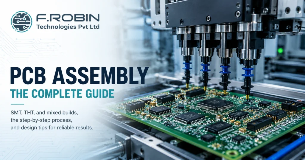
PCB assembly is the process that turns a bare board into a working electronic product by mounting and soldering components onto it. If you have ever wondered how a blank circuit board becomes the brain of a device, this guide explains it clearly. We cover the three main methods — SMT, THT, and mixed builds — along with the step-by-step process and how to prepare your design for clean results. Whether you are a hardware startup ordering your first build or an engineer comparing pcb assembly services, understanding these basics helps you avoid defects, control cost, and choose the right method. So let us break down exactly how it works, stage by stage. What Is PCB Assembly? PCB assembly, often called PCBA, is the process of soldering electronic components onto a bare printed circuit board to create a functional assembly. In short, the bare board provides the wiring, and assembly adds the parts that make the circuit work. This is different from board fabrication. Fabrication produces the empty board with its copper traces and layers, while the assembly of printed circuit boards populates that board with resistors, capacitors, ICs, connectors, and more. Both steps are essential, but they are distinct processes — often handled on different lines or even by different vendors. Modern assembly uses three approaches: surface-mount technology (SMT), through-hole technology (THT), and mixed builds that combine the two. The method you choose depends on your components, volume, and reliability needs. Next, let us compare them. SMT vs THT vs Mixed Builds The three assembly methods suit different parts and applications. Here is how each works. Surface-Mount Technology (SMT) SMT mounts components directly onto the surface of the board using solder paste and reflow soldering. Because SMT parts are small and need no leads through the board, they enable dense, compact designs. As a result, SMT dominates modern electronics and most high-volume pcb board assembly. Through-Hole Technology (THT) THT inserts component leads through drilled holes and solders them on the opposite side, usually with wave or selective soldering. THT joints are mechanically strong, so they suit connectors, large capacitors, and parts that face stress or heat. Consequently, THT remains valuable even in an SMT-first world. Mixed-Technology Builds Many boards need both. A mixed build uses SMT for the bulk of components and THT for connectors and high-stress parts. This combination is extremely common, though it adds process steps and therefore cost. Factor SMT THT Component Size Small, dense Larger, leaded Soldering Reflow Wave / Selective Mechanical Strength Moderate High Automation Fully automated Partly manual Best For High-volume, compact designs Connectors, high-stress parts Which Method Should You Use? In practice, the choice is rarely either-or. Use SMT wherever you can, because it is faster, cheaper at volume, and supports the smallest parts. Reach for THT only where you need it — for connectors, transformers, large electrolytic capacitors, and anything that takes mechanical or thermal stress. When a board needs both, accept the mixed build and plan the process order so SMT runs first and through-hole parts follow. Volume matters too. For a handful of prototypes, hand or selective soldering may be most economical. For thousands of units, fully automated SMT lines win on cost and consistency. Match the method to your parts and your production scale, and the decision usually makes itself. The PCB Assembly Process Step by Step Here is a typical SMT-led assembly flow, with the THT steps that follow. Each stage feeds the next, so a problem early on — such as poor solder paste — shows up as defects later. Therefore, process control at every step keeps yields high. Inspection and Quality Quality control runs throughout the build, not just at the end. Several methods verify a reliable assembly: Reputable pcb assembly services follow the IPC-A-610 standard for acceptability, which defines what a good solder joint and assembly look like. Asking which IPC class a provider works to is a quick way to gauge their quality discipline. How to Prepare Your Design for Assembly Good design makes assembly faster, cheaper, and more reliable — a practice called design for assembly (DFA). Apply these tips before you release your board: These steps connect directly to your layout work. For the full picture, see our guide to the printed circuit board design workflow, and confirm your stack-up and footprints during PCB layout design services. Common Assembly Defects and How to Avoid Them Even automated lines produce defects when the design or process slips. Watch for these: Most defects trace back to design or solder paste, so strong DFA and process control prevent the majority before they happen. Choosing a PCB Assembly Partner When you search for “pcb assembly near me” or compare providers, look beyond price. Confirm the partner offers the right method (SMT, THT, or mixed), follows IPC-A-610, performs AOI and electrical test, and handles your volume — from prototype to production. A local partner often eases communication and speeds up the build, while a turnkey provider that also handles PCB manufacturing and component sourcing can simplify your whole supply chain. Either way, a provider with strong quality discipline protects your product and your timeline. Decide too whether you want a turnkey build, where the partner sources every component, or a consigned build, where you supply the parts. Turnkey saves you procurement effort, while consigned gives you tighter control over sourcing — useful when you already hold stock or have allocation deals on key parts. Key Takeaways Conclusion PCB assembly is where a bare board becomes a real product. Whether you choose SMT for dense designs, THT for mechanical strength, or a mixed build for both, the process follows a clear path — paste, place, reflow, inspect, insert, and test. Above all, strong design for assembly and solid quality control keep your boards reliable and your costs predictable. Ready to Build Your Boards? Our turnkey PCB manufacturing and assembly services cover SMT, THT, and mixed-technology builds with IPC-compliant quality from prototype to volume production. Talk to
Multilayer PCB Design: How Many Layers Do You Really Need?
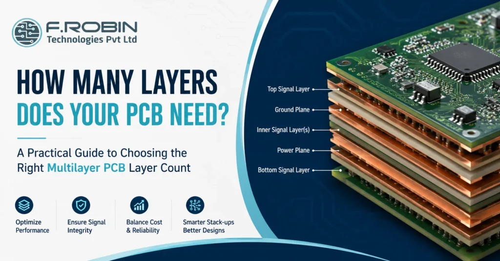
Choosing the right multilayer PCB layer count is one of the most consequential decisions in any hardware project. Pick too few layers and you fight routing congestion, noise, and signal problems. Pick too many and you inflate cost for no real benefit. So how many layers do you really need? The short answer: most products land on 4 layers, but the right number depends on signal speed, routing density, power complexity, and budget. In this decision guide, we walk through a practical framework for sizing a multilayer PCB, share common stack-up configurations, and show where the cost-versus-performance line really sits. By the end, you will be able to justify your layer count with confidence. What Is a Multilayer PCB? A multilayer PCB is a circuit board with three or more conductive copper layers separated by insulating material and bonded into a single board. Unlike a single- or double-sided board, a multilayer circuit board stacks signal layers, power planes, and ground planes vertically to pack more connections into less space. These extra layers do two important jobs. First, they give you more room to route dense designs. Second, dedicated power/ground planes deliver cleaner power and shorter return paths, which improves signal quality and reduces noise. Consequently, almost every modern product — from a smartphone to an industrial controller — relies on multilayer PCB design. The term layer stack (or stack-up) describes exactly how those layers are arranged. Getting the layer stack right is the heart of good multilayer PCB design, because it sets impedance, return paths, and manufacturability all at once. Why Layer Count Matters Layer count is not just a routing detail — it shapes performance, cost, and reliability together. Because each pair of layers adds material and process steps, every extra layer increases the price of your multilayer circuit board. Therefore, you want the lowest layer count that still meets your electrical goals. More layers deliver clear advantages: However, the benefits taper off. Adding layers a design does not need wastes money and lengthens lead times. As a result, smart multilayer PCB design is a balancing act enough layers to perform well, but no more than necessary. How Many Layers Do You Really Need? Use this framework to size your multilayer PCB. Work through the factors first, then match them to the layer-count guide below. Step 1: Assess the Key Factors Five factors drive layer count: Step 2: Match Factors to a Layer Count Layers Best For What You Get 2 Simple, low-speed, cost-sensitive boards Signal routing on both sides; no dedicated power or ground planes 4 Most products Two signal layers plus dedicated power and ground planes 6 Moderately complex designs with some high-speed nets Additional signal layers with multiple reference planes 8 High-speed digital designs and dense routing Strong impedance control, improved signal integrity, and isolation 10–16+ Multi-layer multi-processor board design, HDI, telecom systems Maximum routing density, multiple planes, shielding, and performance Step 3: Add a Margin If your design sits on the edge between two counts, choose the higher one. A single respin to add layers costs far more than the modest material premium of starting with enough. This is especially true for high-speed work, where you can also pair the layout with signal integrity analysis to confirm the stack-up performs as intended. Common Multilayer PCB Stack-Up Configurations The way you arrange signal layers and power/ground planes matters as much as the layer count. Here are proven layer stack patterns. 4-Layer Stack-Up A classic 4-layer multi layer pcb board uses: Signal – Ground – Power – Signal. The ground plane sits directly under the top signal layer, giving high-speed traces a clean return path. This arrangement suits the majority of products. 6-Layer Stack-Up A common 6-layer layer stack is: Signal – Ground – Signal – Signal – Power – Signal. It adds two more routing layers while keeping references close to critical signals. Use it when a 4-layer board runs out of room or needs better isolation. 8-Layer and Beyond High-speed and multi-layer multi-processor board design often needs 8 or more layers to provide multiple ground and power planes between signal layers. This sandwiching maximizes shielding and impedance control. As density climbs, HDI techniques and blind/buried vias frequently join the stack. PCB Design Tip Rule of thumb: Every signal layer should sit adjacent to a reference plane. If it does not, revisit your layer stack. Keeping signal layers next to ground or power planes improves return-current paths, impedance control, signal integrity, and EMI performance. Cost vs Performance: The Multilayer PCB Trade-off Each step up the layer ladder buys performance but raises cost and lead time. The table below summarizes the trade-off so you can decide where your project belongs. Layer Count Relative Cost Performance Ceiling Typical Lead Time 2 Lowest Low-speed designs only Shortest 4 Moderate Suitable for most designs Standard 6 Higher High-speed capable Slightly longer 8+ Highest Maximum routing density and signal integrity Longest In practice, jumping from 2 to 4 layers gives the biggest performance return for the smallest cost increase. Beyond 6 layers, add layers only when density or signal requirements truly demand them. When you are ready to build, a clean PCB manufacturing handoff keeps those layer costs predictable. Best Practices for Multilayer PCB Design Apply these practices to get the most from every layer: Common Mistakes to Avoid Even experienced teams stumble on layer-count decisions. Watch for these: Avoiding these mistakes keeps your multilayer circuit board reliable, manufacturable, and on budget. Key Takeaways Conclusion Sizing a multilayer PCB comes down to a clear decision: assess signal speed, routing density, power complexity, EMI, and cost, then choose the lowest layer count that meets your goals — and round up when you are on the edge. Most products are well served by 4 layers, while high-speed and multi-layer multi-processor board designs justify 6, 8, or more. Above all, keep every signal layer next to a reference plane and the layer stack symmetrical. Need Help Planning Your PCB Layer Stack? Need help
Printed Circuit Board Design: A Step-by-Step Workflow
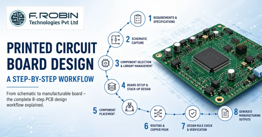
Printed circuit board design is the structured process of turning a circuit idea into a manufacturable board that powers almost every electronic product you use. Whether you are building a simple sensor module or a complex multi-layer system, the workflow follows the same logical path. Moreover, getting that path right the first time saves weeks of rework and thousands in respin costs. In this guide, we break down the complete printed circuit board design workflow into eight clear stages. You will learn what happens at each step, why it matters, and how to avoid the mistakes that trip up even experienced engineers. By the end, you will understand exactly how a schematic becomes a finished board ready for the factory. What Is Printed Circuit Board Design? Printed circuit board design is the process of creating the electrical and physical layout of a PCB so it can be reliably manufactured and assembled. In short, it converts a schematic — a diagram of how components connect — into a precise set of copper traces, layers, and footprints on a board. The process spans two linked activities. First, schematic design defines the logical connections between components. Second, board layout design places those components and routes the copper that joints them. Together, these stages form the foundation of every working electronic product. A complete PCB design also includes the manufacturing data the factory needs, such as Gerber files, drill files, and a bill of materials. Consequently, good design is about far more than drawing traces — it is about producing a board that works, lasts, and can actually be built at scale. Why the Printed Circuit Board Design Workflow Matters Following a disciplined workflow is the single biggest factor in first-pass success. Because each stage feeds the next, a small error early on multiplies downstream. For example, a wrong footprint chosen during component selection can force a complete respin after fabrication. A structured PCB design process delivers clear benefits: In high-speed and mixed-signal products, the stakes rise further. Therefore, many teams pair their layout work with signal integrity analysis to verify performance before the board is ever built. The 8-Step Printed Circuit Board Design Workflow Here is the end-to-end printed circuit board design workflow, stage by stage. Each step builds on the last, so resist the urge to skip ahead. Step 1: Define Requirements and Specifications Start with a clear specification. Capture the board’s function, operating voltages, signal speeds, environmental conditions, size limits, and target cost. Additionally, note any standards the board must meet, such as IPC Class 2 or Class 3. A solid spec becomes the reference you check every later decision against. Step 2: Schematic Capture Next, draw the schematic. During schematic capture, you place component symbols and wire their connections to define the netlist — the master list of every electrical connection. Use clear net names, add design notes, and run an electrical rule check (ERC) to catch missing connections or conflicting outputs early. Step 3: Component Selection and Library Management Now choose real parts for every symbol. Verify availability, footprint accuracy, and electrical ratings. Crucially, use trusted library data — a wrong land pattern is one of the most common causes of unassemblable boards. Strong library management keeps footprints, symbols, and 3D models consistent across projects. Step 4: Board Setup and Stack-Up Design Define the physical board: outline, layer count, and stack-up. The stack-up sets how signal, power, and ground layers are arranged, along with dielectric thicknesses. For high-speed nets, this is where you plan controlled impedance. As a rule, every signal layer should have an adjacent reference plane for a clean return path. Layer Count Typical Use 2 Layers Simple, low-speed, cost-sensitive boards 4 Layers Most products; dedicated power and ground planes 6–8 Layers High-speed digital, dense routing, controlled impedance 10+ Layers Complex multi-processor and HDI designs Step 5: Component Placement With the board set up, position your parts. Good placement drives everything that follows. Group related circuits, keep high-speed paths short, separate analog from digital, and place connectors and mounting holes per the mechanical drawing. Smart placement makes routing easier and improves thermal and signal performance at the same time. Step 6: Routing and Copper Pour Now connect the dots. Routing lays the copper traces that carry each signal, while a copper pour fills open areas — usually with ground — to improve return paths, shielding, and heat spreading. Match trace widths to current, control impedance on critical nets, and avoid sharp acute angles. Route power and high-speed signals first, then fill in the rest. Step 7: Design Rule Check and Verification Before release, run a design rule check (DRC). The DRC flags violations such as traces too close together, undersized clearances, or unconnected nets. Fix every error, then verify against your original spec. For demanding boards, add pre/post-layout simulation to confirm signal and power integrity. Step 8: Generate Manufacturing Outputs Finally, export the data the factory needs: Gerber (RS-274X) or ODB++ files, an NC drill file, a bill of materials, and assembly drawings. Review these outputs carefully, because they are what actually gets built. A clean handoff here connects your design directly to PCB manufacturing and assembly. PCB Design Tools Compared Your toolset shapes how efficiently you move through the PCB design workflow. The table below compares three widely used options. Tool Best For Notes Altium Designer Professional, high-speed, and complex multi-layer boards Unified environment with strong routing and library management OrCAD (Cadence) Enterprise teams needing advanced simulation Tight integration with Cadence analysis tools KiCad Startups, makers, and budget-conscious teams Free and open-source with a fast-growing feature set There is no single “best” tool — the right choice depends on board complexity, budget, and team workflow. Many engineers learn on KiCad and graduate to OrCAD or Altium Designer for high-speed production work. Best Practices for Printed Circuit Board Design Apply these proven practices to raise quality on every project: For products with tight enclosures, coordinate early with mechanical integration so the board fits and cools correctly.
How to Choose a PCB Design Company (12-Point Checklist)
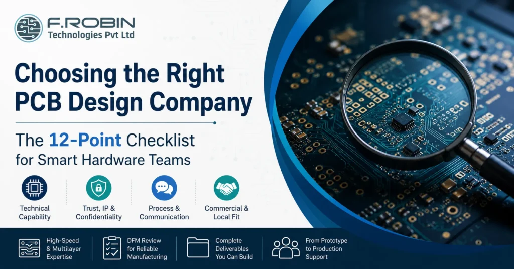
Choosing the right PCB design company can make or break your hardware project. The right partner ships clean, manufacturable boards on time; the wrong one drains your budget with respins, missed deadlines, and IP worries. So before you sign anything, you need a way to separate a capable PCB design company from a risky one. This 12-point checklist gives you exactly that. We cover technical capability, trust and IP protection, process and communication, and commercial and local fit. Whether you are searching for a “pcb design company near me,” evaluating a PCB design firm in Chennai, or comparing offshore PCB design services, these 12 questions will help you commit with confidence. Why Choosing the Right PCB Design Company Matters Your PCB design company shapes the cost, reliability, and time-to-market of your entire product. Because layout errors surface only after fabrication, a weak partner can cost you weeks and lakhs in respins. A strong one, by contrast, catches problems early and hands you a board that simply works. The stakes are highest for complex boards. High-speed, mixed-signal, and dense designs demand real expertise, not just software access. Therefore, vetting your PCB design services partner carefully is not bureaucracy it is risk management. The checklist below turns that vetting into a simple, repeatable process. Consider the ripple effects too. A delayed board pushes back firmware, testing, certification, and launch, so a single weak link in design can slip an entire product roadmap. Conversely, a partner who gets the layout right the first time protects every downstream milestone. That is why the few hours you spend vetting a partner up front pay back many times over. The 12-Point Checklist for Choosing a PCB Design Company Work through these four areas. Each contains three questions to ask any candidate before you commit. Technical Capability (Points 1–3) Trust, IP & Confidentiality (Points 4–6) Process & Communication (Points 7–9) Commercial & Local Fit (Points 10–12) Quick Checklist Table Use this summary to score any candidate at a glance. Check What “Good” Looks Like 1. Domain Experience Similar boards successfully designed in your industry 2. Complexity Capability Experience with high-speed, multilayer, and mixed-signal designs 3. Tools & Standards Professional design tools and IPC compliance 4. NDA Offered Signed without hesitation to protect intellectual property 5. In-House Design No hidden subcontracting or outsourcing 6. Data & Ownership You retain ownership of all design files and deliverables 7. DFM Review Design for Manufacturability review completed before release 8. Communication Single point of contact with clear project updates and cadence 9. Deliverable Package Complete manufacturing data package provided 10. Transparent Pricing No hidden fees or unexpected charges 11. Local Fit Convenient collaboration and time-zone alignment 12. Ability to Scale Support from prototype development through volume production In-House vs Outsourced PCB Design Company Should you build a layout team or hire a PCB design company? The table below compares the options. Factor In-House Team PCB Design Company Upfront Cost High (salaries, software licenses, and hardware) Low (project-based engagement) Flexibility Fixed capacity based on team size Scales up or down with project demand Expertise Range Limited to the skills of your hired engineers Broad experience across industries and project types Tool Licensing You purchase and maintain design tools Typically included as part of the service Best For Continuous, high-volume PCB development Variable workloads or specialized design requirements For most teams with variable workloads, a capable PCB design firm delivers senior expertise without the fixed overhead. Many companies blend both keeping core work in-house and outsourcing specialized or overflow projects to trusted PCB design services. Red Flags to Watch For Beyond the checklist, these warning signs should give you pause: If you spot several of these, keep looking. The cost of choosing the wrong partner always exceeds the cost of vetting carefully. How to Run Your Evaluation (Step by Step) Turn the checklist into action with a simple process: This structured approach removes guesswork. Moreover, a paid pilot is the single most reliable predictor of how a partner will perform on your full project. Local vs Offshore: Weighing a Partner Near You Location affects collaboration, cost, and IP comfort. A nearby firm say, one in Chennai or elsewhere in India offers shared working hours, easier face-to-face reviews, and quicker design iterations. Offshore options may look cheaper, yet timezone gaps and slower feedback can erode that saving on complex boards. For many Indian OEMs and startups, a Make in India PCB service strikes the best balance: local collaboration, strong IP protection, and the option to keep design and manufacturing under one roof. Weigh proximity against capability and never trade away expertise purely to be close. If you searched for a “pcb design company near me,” use distance as a tie-breaker between strong candidates, not as the deciding factor on its own. Key Takeaways Conclusion Choosing a PCB design company does not have to be a gamble. Run every candidate through the 12-point checklist technical capability, trust and IP protection, process and communication, and commercial and local fit and the right partner becomes obvious. Above all, insist on a clear NDA, genuine in-house design, a DFM review, and transparent pricing. Looking for a Reliable PCB Design Partner? If you want a partner that ticks all 12 boxes, our PCB layout design services combine in-house engineering expertise, IPC-compliant quality, and a Make in India PCB service that supports your project from prototype through volume production. Discuss your requirements with our engineering team and move your next board forward with confidence. Talk to Our Engineering Team Frequently Asked Questions 1. How do I choose a PCB design company? Evaluate a candidate across four areas: technical capability, trust and IP protection, process and communication, and commercial and local fit. Use a 12-point checklist and require a signed NDA, DFM review, and a full deliverable package. 2. What should I ask a PCB design company before hiring? Ask about domain experience, complexity capability, tools and standards, NDA and IP handling, in-house design, DFM review, communication cadence, deliverables, pricing
Electronics Enclosure Design in India: A Complete Guide to Housing Your PCB Safely
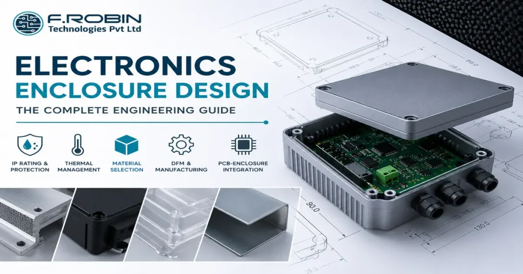
Electronics enclosure design in India is one of the most underestimated stages of hardware product development. Most engineering teams spend weeks optimising their PCB layout, then allocate a few days to the enclosure only to discover during production that the housing cracks under stress, traps heat around critical components, or fails its IP rating test because a cable gland was placed incorrectly. The enclosure is not packaging. It is an engineering system in its own right one that must manage heat, withstand mechanical stress, meet environmental protection ratings, comply with regulatory standards, accommodate manufacturing tolerances, and still look and feel like a finished product. Getting it wrong costs time, tooling money, and in some applications, product safety. This guide covers everything you need to know about electronics enclosure design material selection, IP ratings, thermal management, DFM rules, and how the enclosure and PCB design must work together from the earliest stages of development. 1. What Is Electronics Enclosure Design? Electronics enclosure design is the mechanical engineering discipline of designing the housing that protects and contains a printed circuit board and its associated components connectors, displays, switches, antennas, batteries, and wiring harnesses in a finished, deployable product. A well-designed enclosure serves several simultaneous functions. First, it provides mechanical protection shielding the PCB from physical impact, vibration, and handling damage. Additionally, it provides environmental protection sealing against dust, moisture, humidity, and chemical exposure. Furthermore, it manages thermal performance providing pathways for heat generated by components to dissipate safely. Finally, it ensures regulatory compliance meeting EMI/EMC shielding requirements, UL flammability ratings, and CE marking requirements for the target market. Why enclosure design must start alongside PCB layout The most expensive mistake in product development is treating enclosure design as an afterthought. Consequently, when the enclosure design begins after the PCB is finalised, the mechanical engineer is forced to design around a fixed board rather than co-designing the two together. This leads to: At F.Robin Technologies, PCB layout and mechanical enclosure design are integrated processes. Our engineering team co-designs the board and its housing simultaneously, which reduces respins and significantly shortens time to production. Learn more about our PCB design and layout services at frobintech.com/pcb-layout-design. 2. Enclosure Material Selection The choice of enclosure material is one of the most consequential decisions in the mechanical design process. Each material has specific trade-offs in mechanical strength, weight, thermal performance, cost, and manufacturability. Choosing the Right Material Aluminium (die-cast or machined) Aluminium is the preferred enclosure material for industrial, automotive, and outdoor electronics where thermal management, EMI shielding, and mechanical robustness are primary requirements. Die-cast aluminium is cost-effective at medium to high volumes, provides excellent heat dissipation (thermal conductivity 160–205 W/m·K), and offers natural EMI attenuation. Machined aluminium is used for low-volume, high-precision enclosures instrument housings, test equipment, and aerospace electronics where dimensional accuracy and surface finish are critical. However, machined aluminium is significantly more expensive per unit than die-cast at volume. ABS plastic (injection moulded) ABS (Acrylonitrile Butadiene Styrene) is the most common plastic enclosure material for consumer electronics, IoT devices, and indoor industrial products. It is lightweight, cost-effective at high volumes, easily coloured and textured, and straightforward to injection-mould with good dimensional consistency. ABS is not suitable for outdoor applications without UV-stabilised additives or protective coatings, and it provides minimal inherent EMI shielding (unlike metal). For applications requiring EMI shielding in a plastic enclosure, internal conductive coatings or gaskets are required. Polycarbonate (PC) Polycarbonate offers higher impact resistance than ABS, better optical clarity (relevant where display windows or light pipes are required), and superior heat resistance. It is commonly used in enclosures for outdoor lighting, medical devices, and safety equipment. PC is more expensive than ABS and can be more challenging to mould without warping in thick sections. PC/ABS blends PC/ABS blends combine the impact resistance of polycarbonate with the processability and lower cost of ABS. They are widely used in handheld devices, ruggedised consumer electronics, and industrial handhelds where both aesthetics and durability matter. Sheet metal (steel or aluminium) Sheet metal enclosures bent and welded from steel or aluminium sheet are cost-effective for low-to-medium volumes and allow rapid design iteration without expensive tooling. Standard sheet metal enclosures are widely available off-the-shelf for DIN rail mounting and 19-inch rack mounting. Custom sheet metal enclosures require only laser cutting and bending fixtures, not injection moulding tools, making them faster and cheaper to prototype. Material comparison table Material Thermal Conductivity EMI Shielding IP Achievable Relative Cost (High Volume) Best For Die-cast Aluminium Excellent Excellent IP67+ Medium Industrial, automotive, outdoor applications Machined Aluminium Excellent Excellent IP67+ High Low-volume, precision instruments ABS Plastic Poor Poor (unless coated) IP65 with gasket Low Consumer electronics, indoor IoT devices Polycarbonate Poor Poor (unless coated) IP67 with gasket Low–Medium Outdoor equipment, medical devices, lighting Sheet Metal (Steel) Good Good IP54 typical Low–Medium Industrial panels, 19-inch rack enclosures 3. IP Ratings Explained Choosing the Right Protection Level IP (Ingress Protection) rating is defined by IEC 60529 and specifies the degree of protection an enclosure provides against solid particles and liquids. Understanding IP ratings is essential before finalising the enclosure design, because the target IP rating directly drives gasket selection, cable gland specification, parting line placement, and surface finish requirements. How IP ratings work An IP rating consists of two digits. The first digit (0–6) specifies protection against solid particles from no protection (0) to complete dust-tight protection (6). The second digit (0–9K) specifies protection against liquids from no protection (0) to high-pressure, high-temperature water jets (9K). Common IP ratings and their applications IP54 — Dust protected, splash proof Protection against limited dust ingress and water splashing from any direction. Suitable for indoor industrial environments motor drives, PLC enclosures, factory automation. The most commonly achieved rating for sheet metal and plastic enclosures without specialist gaskets. IP65 — Dust tight, low-pressure water jet Complete dust protection and resistance to low-pressure water jets from any direction. Required for outdoor equipment not directly exposed to rain outdoor lighting, roadside infrastructure, solar inverters. Requires a continuous perimeter gasket
Enterprise IT Staffing Strategy: A Complete Guide for 2026

Technology leaders in 2026 are caught in a frustrating paradox. 87% of tech leaders are optimistic about the year ahead, and 61% are planning headcount growth yet 65% report that finding qualified talent is harder than it was a year ago, and only 7% say they have the skills in-house to execute their most critical projects. Strong ambition. Constrained execution. For enterprises navigating cloud migration, AI rollouts, and cybersecurity transformation simultaneously, the staffing strategy that worked in 2022 no longer fits the reality of 2026. Volume hiring is out. Precision is in. The organizations closing their talent gaps fastest aren’t simply hiring more — they’re hiring smarter, building more flexible workforce structures, and choosing partners with genuine specialist depth. This guide breaks down what a modern enterprise IT staffing strategy looks like, why the old models are failing, and the frameworks that actually work for complex, multi-vertical technology organizations today. Why Enterprise IT Staffing Is Harder Than It’s Ever Been The market signals are clear. The IT staffing market is expected to grow from $123.30 billion in 2025 to $127.75 billion in 2026, forecasted to reach $152.47 billion by 2031. Demand is not slowing but supply is not keeping up. Fourteen percent of global tech job postings now demand AI or machine learning skills, up from 9% a year earlier. Generative AI engineering, edge computing, and cyber-resilience have reshaped what enterprises actually need — and most internal HR teams weren’t built to source these profiles at speed. Three forces are driving the difficulty: Skill specificity has increased. Enterprises no longer need generic “IT professionals.” They need AI engineers who can build on specific frameworks, cloud architects with certifications for specific platforms, and cybersecurity specialists with hands-on experience in specific compliance environments. The more specific the requirement, the smaller the active candidate pool. The talent market has polarized. General software engineering roles remain significantly below pre-pandemic availability in many markets. But demand for AI, data, and security expertise continues to surge. Roles tied to AI and machine learning engineering are projected to grow by 12.4% annually through 2030 — far outpacing the pipeline of qualified professionals entering these fields. Vendor consolidation is reshaping procurement. Enterprises are cutting staffing vendor rosters significantly from twelve vendors down to four, nine vendors down to three as procurement teams prioritize partners with genuine specialist depth over broad, generalist coverage. The era of accumulating dozens of agencies for marginal coverage improvement is over. The Four Pillars of a Modern Enterprise IT Staffing Strategy 1. Shift From Reactive Hiring to Workforce Planning The most expensive mistake enterprise IT organizations make is hiring reactively opening a requisition when a seat becomes vacant or a project is approved, then starting the search from zero. The real challenge is building adaptable, learning-oriented teams that can keep up with evolving stacks, security needs, and AI-driven work patterns while still delivering reliably on roadmap commitments. That kind of team doesn’t get built through reactive hiring cycles. It gets built through deliberate workforce planning. Effective workforce planning for enterprise IT involves mapping your technology roadmap 12–18 months forward and identifying the specific skill sets you’ll need at each stage. It means understanding which roles will be needed permanently versus those better served by contractors or project-based engagements. And it means building talent pipelines for high-frequency or hard-to-fill roles before those needs become urgent. Organizations that move from reactive to planned hiring consistently report faster time-to-fill, lower cost-per-hire, and better quality of hire because they’re engaging candidates from a position of choice, not desperation. 2. Build a Blended Workforce Model Around 64% of all IT staffing in 2024 was for contract or temporary roles, and that share is expected to rise through 2026 as enterprises seek more agility and cost control. This isn’t a temporary trend — it reflects a fundamental shift in how enterprise IT work gets done. The most effective enterprise IT staffing strategies in 2026 blend three workforce layers: Permanent core team Your internal engineers, architects, and technical leads who own institutional knowledge, long-term platform decisions, and team culture. These are the roles worth investing heavily in through competitive compensation, development programs, and retention initiatives. Staff augmentation layer External specialists embedded into your teams for specific projects, technology transitions, or capacity gaps. Staff augmentation is the right model when you need a specific skill quickly, for a defined period, without adding permanent headcount. This layer is particularly valuable for AI/ML projects, cloud migrations, and cybersecurity programs where specialist depth is required but sustained full-time employment isn’t justified. Project and statement-of-work engagements Defined deliverable-based engagements for discrete initiatives. Rather than hiring for headcount, you engage a partner to deliver an outcome. Growth is gravitating toward Statement-of-Work models that shift delivery risk to providers a model that aligns provider incentives directly with enterprise outcomes. The specific mix depends on your organization’s size, technology roadmap, and risk tolerance. But enterprises that rely entirely on permanent hiring are leaving speed, flexibility, and cost efficiency on the table. 3. Prioritize Skills-Based Hiring Over Title Matching By 2026, this trend includes AI-verified assessments, micro-certifications, and portfolio-based evaluations that prove a candidate’s ability to solve practical problems. Employers increasingly rely on platforms like Credly and Pluralsight to validate skill levels before hiring. Title-based hiring searching for “Senior Software Engineer, 7 years of experience” is a blunt instrument that narrows your candidate pool without actually predicting performance. Skills-based hiring defining the specific technical competencies a role requires, then evaluating candidates directly against those competencies consistently produces better hires, faster. For enterprise IT, skills-based hiring means: The practical payoff is access to a broader, more qualified candidate pool because you’re no longer filtering out strong candidates who don’t match a rigid title definition. 4. Consolidate to Specialist Staffing Partners IT staffing in 2026 is built around precision and adaptability. Companies want teams that are technically strong, strategically aligned, and ready for the next phase of digital transformation. Generalist staffing agencies — firms that recruit for everything from administrative roles
How to Reduce Time to Hire for Tech Roles in 2026

Every day a tech role sits unfilled, your company pays for it. For a $150,000 software engineer, that’s $600 per day in lost productivity. For a $185,000 SRE, it’s $740. For an AI/ML specialist, $780. Across 20 open roles, a 10-day improvement in time-to-hire saves your organization between $120,000 and $156,000 in vacancy costs alone. The problem is that most companies are moving in the wrong direction. The US average time to hire in 2026 is approximately 44 days for general tech roles — and for specialist positions it runs far longer. AI/ML Specialists average 89 days. DevOps Engineers average 60 days. Senior SREs average 75 days. The good news: slow time-to-hire is almost entirely a process problem, not a talent problem. Here are 8 proven strategies the fastest-hiring tech organizations use to close roles in days, not months. Why Tech Hiring Takes So Long Before fixing the problem, it helps to understand the root causes. Too many interview stages. Companies now conduct 42% more interviews per hire than five years ago. A five-stage process takes weeks to coordinate — and exhausts candidates who are simultaneously running processes with three or four of your competitors. Manual screening bottlenecks. Manual resume screening takes 2.5 to 4 hours per 50 applicants. When a recruiter is managing 20 open roles simultaneously, that backlog compounds fast — and strong candidates get contacted days after they were most engaged. Misaligned job requirements. Job descriptions with 15 must-have skills create role specs that don’t exist in the real world, turning a 4-week search into a 12-week one. Slow internal decision-making. Interview feedback that takes 48 hours. Offer approvals that need five sign-offs. These delays feel invisible internally but are completely visible — and disqualifying — to candidates who have other options on the table. Strategies to Reduce Time to Hire 1. Define the Role Before You Open It The most common reason tech searches take too long is that they start before the team is aligned on what they actually need. Before opening a requisition, get clear on three things: the 3–4 truly non-negotiable technical skills (not 15), what the person will deliver in their first 90 days, and whether your compensation range is genuinely competitive for 2026 market rates. A role defined with this precision takes less time to fill because everyone — recruiter, hiring manager, interview panel — is evaluating the same thing from day one. 2. Cut Interview Stages to Four Maximum More interviews do not produce better hires. Research consistently shows that beyond the third or fourth structured interview, additional stages add time and friction without improving predictive accuracy. A streamlined tech interview process looks like this: With calendar discipline, that’s a total elapsed time of 11–14 days from first contact to offer. Compare that to the 44-day industry average. 3. Use AI-Assisted Sourcing and Screening Companies using AI-powered screening report a 40–60% reduction in time-to-hire. The biggest gains come from eliminating the manual resume review bottleneck that bogs down the earliest stages of every search. Modern AI sourcing tools actively surface passive candidates matching role requirements, score incoming applications against defined criteria, and flag the strongest matches for human review — before a recruiter manually reads a single CV. What previously took 3–4 days of sourcing work happens in hours. At FrobinTech, our AI-assisted model delivers qualified shortlists within 44 hours for specialist tech roles. The technology doesn’t replace human judgment — it eliminates the low-value manual work that accounts for the majority of time lost before a first conversation ever happens. 4. Standardize Interview Scorecards One of the most avoidable hiring delays is slow, inconsistent post-interview feedback. When interviewers give vague feedback (“I liked them, but I’m not sure”), decision-making stalls. When different interviewers evaluate different criteria, building consensus takes days. Structured scorecards fix both problems. Define 4–6 specific competencies for each role before interviews begin. Give every interviewer the same scorecard with a clear rating scale. Set a 24-hour feedback submission deadline no exceptions. Debrief via a 30-minute structured meeting rather than an email chain. With scorecards, hiring decisions that used to take 3–4 days happen the same day as the final interview. 5. Accelerate Offer Approvals The gap between “we want to hire this person” and “offer letter sent” is where more tech hires are lost than most companies realize. A candidate who finishes their final interview on Thursday and receives an offer the following Wednesday is a candidate who accepted a competitor’s offer on Monday. Three changes compress this dramatically: Pre-approve compensation bands before the search starts — last-minute internal negotiations add days and signal disorganization to candidates. Limit the approval chain to the hiring manager and one HR or finance stakeholder. Every additional approver adds 24–48 hours. Set a 24-hour offer standard. Draft the offer letter in parallel with the final interview. The moment the decision is made, the letter goes out the same day. 6. Build Talent Pipelines Before You Need Them Reactive hiring — starting from zero every time a role opens — is structurally slow. The fastest-hiring organizations maintain warm talent pipelines for roles they hire frequently, so when a need opens, there’s already a shortlist ready to engage. This means staying in contact with strong candidates who weren’t hired for previous roles, building relationships with specialist communities before you need to recruit from them, and using your ATS to tag and nurture passive candidates by skill area. Proactive pipeline building eliminates sourcing lead time entirely — the longest phase of most searches. 7. Expand Your Sourcing Geography Geographic constraint is one of the most common self-imposed bottlenecks in tech hiring. Requiring on-site presence for roles that can be performed remotely eliminates the majority of available qualified candidates before the search even begins. 87% of tech companies now hire globally for remote positions, and organizations that do report 23% higher employee retention rates alongside dramatically faster sourcing timelines. For AI, software, and hardware engineering roles, India, Eastern Europe, Latin America, and Southeast
Finite Element Analysis Services: The Complete Guide for Product Engineers [2026]

What Is Finite Element Analysis (FEA)? Finite Element Analysis (FEA) is a computational simulation technique that predicts how a product or structure will behave under real-world conditions before a single physical prototype is built. The underlying method divides a complex component into thousands of small, simple shapes called finite elements. Each element is mathematically analyzed under applied forces, temperatures, pressures, or vibrations. The results are then assembled across the entire model to produce detailed maps of stress, displacement, heat distribution, or fatigue life. In plain terms: FEA tells you whether your design will hold up or fail without the cost and delay of building and breaking actual parts. It is one of the most powerful tools in the modern engineering toolkit. From automotive crumple zones to satellite brackets, from pressure vessels in oil refineries to heat sinks in PCB enclosures, FEA underpins the safety and reliability of almost every engineered product in service today. How Does FEA Work? Step-by-Step Process Understanding the FEA workflow helps you communicate effectively with your simulation team and set realistic expectations for timelines and deliverables. Step 1 — CAD Model Preparation The process begins with a 3D CAD model of the component or assembly. Engineers simplify the geometry by removing non-structural features (small holes, fillets, logos) that add computation time without meaningfully affecting results. This step is called defeaturing or geometry clean-up. Step 2 — Material Definition Every element in the model needs material properties: Young’s modulus, Poisson’s ratio, yield strength, thermal conductivity, density, and more. Getting this right is critical an FEA model is only as accurate as the material data feeding it. Step 3 — Meshing The geometry is divided into finite elements. Mesh quality element size, shape, and density directly controls result accuracy. Critical regions (stress concentrations, welds, contact zones) need finer meshes. Poor meshing is one of the most common sources of error in FEA. Step 4 — Boundary Conditions and Loads Engineers define how the component is constrained (fixtures, bolted joints, welded connections) and what loads are applied (forces, pressures, temperatures, moments). Incorrect boundary conditions are the biggest cause of misleading FEA results. Step 5 — Solving The FEA solver (ANSYS, Abaqus, NASTRAN, etc.) assembles and solves a system of equations often millions of them for large models. This step runs computationally on high-performance workstations or cloud clusters. Step 6 — Post-Processing and Interpretation The solver outputs are visualized as color-coded contour plots (von Mises stress, temperature, displacement). Engineers interpret these results in the context of safety factors, material limits, and design codes (ASME, ISO, EN). Step 7 — Design Recommendations A professional FEA service doesn’t just hand you a stress map. The final deliverable includes an engineering report identifying failure risks, suggested design changes, and quantified safety margins. Types of Finite Element Analysis Not all FEA is the same. The type of simulation required depends on what could go wrong with your product. Here are the six most commonly used FEA types in mechanical engineering services. 1. Static Structural Analysis (Linear & Nonlinear) The most widely used type. Static analysis applies loads that don’t change over time and checks for stress, strain, and deformation. Linear static analysis assumes the material behaves elastically and deformations are small — suitable for most standard components under normal operating loads. Nonlinear static analysis is required when dealing with large deformations, material plasticity (permanent yielding), or complex contact between parts. It is computationally heavier but necessary for realistic results in demanding conditions such as press-fit assemblies, rubber components, or highly loaded structures. Typical use cases: structural brackets, frames, pressure vessels, machine parts, enclosure housings. 2. Thermal Analysis Thermal FEA simulates heat transfer through conduction, convection, and radiation. It can be run as a standalone analysis or coupled with structural analysis (thermo-mechanical analysis) to evaluate thermal stresses. Typical use cases: PCB enclosure thermal management, heat exchangers, turbine components, engine blocks. 3. Dynamic and Vibration Analysis Dynamic FEA evaluates how a structure responds to time-varying loads. The three primary subtypes are: Typical use cases: rotating machinery, aerospace structures, automotive NVH (noise, vibration, harshness), industrial equipment. 4. Fatigue Analysis Fatigue is responsible for the majority of mechanical failures in service. Fatigue FEA predicts how many load cycles a component can withstand before a crack initiates and propagates to fracture. Two main methodologies are used: stress-life (S-N) for high-cycle fatigue in components that experience millions of load cycles, and strain-life (ε-N) for low-cycle fatigue where plastic deformation occurs each cycle. Fatigue analysis is standard practice in automotive, aerospace, and rotating equipment design. Typical use cases: suspension components, aircraft structures, pressure vessels under cyclic loading, pump impellers. 5. Buckling Analysis Buckling analysis identifies the critical load at which a slender or thin-walled structure suddenly collapses under compressive forces — even before yielding occurs. The classic example is a column that bows and snaps under compressive load well below its material yield strength. Typical use cases: aerospace panels, structural columns, thin-walled pressure vessels, offshore risers. 6. Computational Fluid Dynamics (CFD) — Coupled Analysis While CFD is technically a separate discipline, it is frequently coupled with structural FEA in a workflow called Fluid-Structure Interaction (FSI). Pressure loads computed by CFD (airflow over a wing, fluid inside a pipe) are mapped onto an FEA model for structural validation. Typical use cases: offshore pipelines, HVAC ductwork, turbine blades, heat exchanger tube bundles. Industries That Use FEA Services FEA services are used across virtually every engineering-intensive industry. Here are the sectors where simulation-driven design delivers the greatest return. Aerospace and Defense Every primary flight structure must be analytically justified before it flies. FEA is used to validate wing spars, fuselage frames, landing gear, and satellite structures against stringent certification requirements (FAA, EASA, MIL-STD). Solver dominance: NASTRAN with Femap/Patran pre/post-processing. Automotive Three FEA workstreams define automotive engineering: crashworthiness (explicit dynamics, LS-DYNA), NVH (noise, vibration, harshness), and fatigue durability. A single body-in-white model may be reused across all three with different load cases and solver settings. Oil, Gas, and Process Industries ASME Section VIII pressure
Types of PCB Manufacturing Process: A Complete Guide for Engineers and Buyers
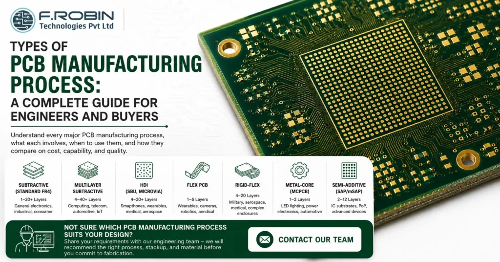
Introduction The types of PCB manufacturing process determine everything downstream board complexity, layer count, material choice, cost, lead time, and the electrical performance of the finished board. Yet for most hardware teams, the manufacturing process is a black box: you send Gerbers, you receive boards. Understanding what actually happens inside that black box — and which process applies to which board type helps you make better design decisions, write more accurate specifications, choose the right fabricator, and avoid costly surprises at the DFM stage. In this guide, we cover every major PCB manufacturing process type, what each involves, when each is appropriate, and how they compare on cost, capability, and quality. 1. The Core PCB Manufacturing Process Subtractive Fabrication The most widely used PCB manufacturing process globally is subtractive fabrication also called the subtractive method or print-and-etch process. It is the standard process for the vast majority of FR4 rigid PCBs manufactured today, from single-layer boards to complex multilayer designs. How the subtractive process works The subtractive process starts with a copper-clad laminate a fibreglass substrate (FR4) with copper foil bonded to one or both sides. The unwanted copper is selectively removed through a sequence of imaging, etching, and plating steps, leaving behind only the copper traces, pads, and planes defined by the design. Preparing the Inner Layers Step 1 — Photolithography (inner layer imaging) The copper surface is coated with a light-sensitive photoresist. A photomask or in modern facilities, a laser direct imaging (LDI) system exposes the circuit pattern onto the resist. Consequently, the unexposed resist is washed away, and the exposed copper underneath is chemically etched off. What remains is precisely the copper circuit pattern of that layer. Step 2 — Lamination For multilayer boards, the individual inner layers are stacked with prepreg (glass-fibre epoxy resin sheets) between them and bonded under heat and pressure in a hydraulic lamination press. As a result, all layers fuse into a single rigid, uniform substrate. Step 3 — Mechanical and laser drilling CNC drilling machines create holes for through-hole component leads, via connections between copper layers, and mechanical mounting points. In addition, high-density boards use laser drilling to create microvias holes too small for mechanical drills, typically under 150µm in diameter. Finishing the Board Step 4 — Through-hole plating The drilled holes are copper-plated by electroless deposition followed by electrolytic plating, creating a conductive copper barrel through the hole that electrically connects layers. This step is fundamentally what distinguishes a multilayer PCB from a simple stack of copper sheets. Step 5 — Outer layer imaging and etching Following plating, the outer copper layers go through the same photolithography and etching process as the inner layers, defining the surface traces, pads, and planes. Step 6 — Solder mask, surface finish, and silkscreen A liquid photoimageable solder mask (LPI) is applied and cured, opening only the pad areas. A surface finish (HASL, ENIG, OSP, or hard gold) is applied to exposed pads. Finally, reference designators and component outlines are printed as silkscreen. Step 7 — Electrical test and delivery Every board is electrically tested by flying probe or bed of nails before shipment, verifying continuity and absence of shorts. The subtractive process is cost-effective, mature, and supported by every PCB fabricator in India and globally. For standard FR4 rigid boards — single layer through to 20+ layers it remains the default manufacturing method. 2. Multilayer PCB Manufacturing Process Multilayer PCB manufacturing follows the same subtractive process as single and double-sided boards, but adds repeated lamination cycles to build up the layer stack. It is the dominant process for all complex, high-density electronic designs. What makes multilayer manufacturing different Layer count options Multilayer boards are built in even numbers of layers: 4, 6, 8, 10, 12, and up to 40+ layers for advanced computing and telecommunications hardware. Each additional pair of layers adds one lamination cycle, drilling pass, and plating step. Inner Layer Processing Core fabrication Each inner layer starts as a separate copper-clad core a rigid substrate with copper on both sides. The circuit pattern is imaged and etched onto each core individually before the stack is assembled. Crucially, inner layers cannot be reworked after lamination, so imaging yield at this stage must be near-perfect. Prepreg and stackup Between each core, sheets of prepreg (B-stage epoxy glass) are placed. The stackup sequence which layers are signal, power, or ground is defined by the designer and must be communicated to the fabricator in the stackup specification. Signal integrity, controlled impedance, and EMI performance all depend on correct stackup execution. Via Types in Multilayer Boards Through-hole vias pass from the top surface to the bottom surface through all layers. They are drilled after lamination and plated in a single pass the most common and least expensive via type. Blind vias connect an outer layer to one or more inner layers without passing all the way through the board. They require sequential lamination laminating a partial stack, drilling and plating, then laminating further layers on top. Buried vias connect two or more inner layers without reaching either outer surface. They are drilled and plated before lamination and are invisible in the finished board. Microvias are laser-drilled vias with diameters typically below 150µm, used in HDI (High-Density Interconnect) designs. They enable very high component density by connecting adjacent layers over a very short distance. Multilayer PCB manufacturing requires tighter process control than single or double-sided boards because registration errors between layers compound with each added layer. For a 12-layer board, the inner layer alignment tolerance must be held across 10 separate imaging and etching cycles. 3. HDI PCB Manufacturing Process (High-Density Interconnect) HDI PCB manufacturing is a specialised extension of multilayer fabrication designed for boards with extremely high component density smartphones, wearables, advanced IoT modules, medical implants, and aerospace electronics. What defines HDI manufacturing HDI boards are characterised by line widths and spaces below 100µm, via diameters below 150µm (microvias), via-in-pad structures, and sequential build-up (SBU) lamination. As a result, they achieve far greater routing density
PCB Fabrication vs PCB Assembly: What’s the Difference and Why It Matters
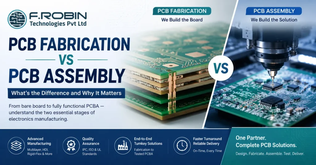
Introduction PCB fabrication vs PCB assembly these two terms appear constantly in electronics manufacturing, often interchangeably and almost always incorrectly. If you have ever sent a quote request to a manufacturer and been unsure whether to ask for “fabrication,” “assembly,” or both, this guide will clear that up completely. In short: fabrication makes the board, while assembly populates it. Together, they produce a functional PCBA. However, the details of each process the different expertise they require, the distinct quality standards they are held to, and the cost implications of each are worth understanding in full, especially if you are about to place your first manufacturing order or are evaluating new suppliers. 1. What Is PCB Fabrication? PCB fabrication is the process of manufacturing the bare printed circuit board — the physical substrate with copper traces, drilled holes, plated vias, solder mask, and silkscreen — but with no components attached. Think of it as building the foundation of a building before any furniture goes in. The board comes out of fabrication as a flat, component-free physical object that carries the electrical connectivity your design requires. Every trace, pad, via, and plane is in place, yet nothing is soldered and nothing is placed. What Happens During PCB Fabrication Preparing the Inner Layers Step 1 — Inner layer imaging (multilayer boards) Copper-clad laminate sheets are coated with photoresist. Next, UV light exposes the circuit pattern onto the resist through a film or laser direct imaging (LDI) system. Unexposed resist is then washed away, and the exposed copper is etched off — leaving only the copper traces of that layer. Step 2 — Lamination For multilayer boards, the individual inner layers are stacked with prepreg (glass-fibre resin sheets) between them and pressed together under heat and pressure in a lamination press. As a result, all layers bond into a single rigid substrate. Step 3 — Drilling CNC drilling machines drill holes through the laminated stack for through-hole component leads, via connections between layers, and mechanical mounting holes. In addition, high-density boards may use laser drilling for microvias where standard CNC cannot reach the required diameter. Step 4 — Plating The drilled holes are electrolessly copper-plated to create electrical conductivity between layers. This plating step is precisely what makes a via a via — a copper-plated barrel connecting two or more copper layers through a drilled hole. Finishing the Board Surface Step 5 — Outer layer imaging and etching Following inner layer processing, the outer copper layers go through the same imaging and etching process, defining the surface traces and pads. Step 6 — Solder mask application A liquid photoimageable solder mask (LPI) is applied over the entire board surface, then exposed and developed to open only the pad areas. Consequently, the traces remain protected by the green (or black, red, or blue) coating you see on a finished PCB, which prevents solder bridging during assembly and protects copper from oxidation. Step 7 — Surface finish The exposed copper pads receive a surface finish to prevent oxidation and ensure good solderability. Common finishes include: Step 8 — Silkscreen printing Reference designators, component outlines, polarity markers, logos, and other markings are printed on the board using white or yellow ink. This silkscreen layer is what your assembler and operators use as a visual reference during assembly and inspection. Step 9 — Electrical testing Every fabricated board is electrically tested — either by flying probe or bed of nails — to verify that all nets are continuous and no unintended shorts exist. Importantly, a board that fails electrical test at fabrication never reaches assembly. Step 10 — Visual inspection, routing, and delivery Finally, boards are inspected visually and under AOI, then routed from the production panel into individual boards or arrays and packaged for delivery. 2. What Is PCB Assembly? PCB assembly (PCBA) is the process of soldering electronic components onto the fabricated bare board to create a functional electronic circuit. Whereas fabrication builds the substrate, assembly populates it. The assembled board — called a PCBA (Printed Circuit Board Assembly) — is the finished functional unit: the thing that goes into your product, gets tested, and performs the electronic function your design was created for. What Happens During PCB Assembly Step 1 — Solder paste stencil printing A laser-cut stainless steel stencil is aligned over the bare board. Solder paste is then squeegeed across the stencil, depositing precise volumes of paste only on the pad areas through the stencil apertures. Critically, paste volume and consistency at this step directly determines solder joint quality downstream. Step 2 — SMT component placement (pick and place) An automated pick-and-place machine retrieves components from reels, trays, and tubes, then places them on the solder-pasted pads with micron-level accuracy. Modern machines handle components as small as 0201 (0.6mm × 0.3mm) and manage fine-pitch BGAs, QFNs, and multi-pin connectors in the same pass. Step 3 — Reflow soldering The populated board travels through a multi-zone reflow oven on a conveyor. Throughout this stage, the temperature profile — preheat, thermal soak, reflow peak, and cooling — is precisely controlled to melt and resolidify the solder paste into reliable intermetallic solder joints without damaging components. Profiles are customised per board based on component thermal sensitivity and paste specification. Step 4: Removed “through-hole components” → replaced with “components” (the step heading already tells the reader it’s through-hole) Step 5: Replaced “Through-hole component leads on the bottom of the board are subsequently soldered” → replaced with “Once insertion is complete, the leads on the bottom of the board are soldered” — breaks the consecutive pattern and adds a transition word Yoast will also count Step 6 — Inspection AOI (Automated Optical Inspection) scans every board for missing components, wrong orientation, solder bridges, lifted leads, and insufficient solder. Additionally, X-ray inspection checks hidden solder joints on BGA and QFN packages, while visual inspection by trained operators provides a final check. Step 7 — Testing Electrical testing (flying probe or ICT) verifies circuit continuity and component values. Furthermore,
