
High Density Interconnect (HDI) PCB Design Explained: Worth It?
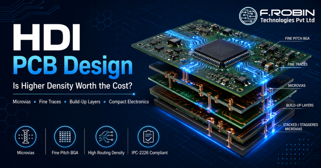
High density interconnect (HDI) PCB design packs more circuitry into less space than a conventional board, using microvias, finer traces, and tighter spacing. As electronics shrink and components grow more complex, HDI has moved from a niche option to a mainstream necessity. But it also costs more — so the real question is whether high-density design is worth it for your product. This guide explains HDI PCB design in plain terms: what it is, the key technologies behind it, when it pays off, and the design rules that keep it reliable. Whether you are designing a compact wearable or a dense processor board, you will learn when a high density interconnect approach is the right call. What Is HDI PCB Design? High density interconnect PCB design is an approach that achieves higher wiring density than standard boards through microvias, fine lines, and thin build-up layers. In short, it lets you route far more connections in the same area — or fit the same circuit into a much smaller board. An HDI circuit board uses laser-drilled microvias instead of large mechanically drilled holes, along with finer traces and tighter spacing. These features free up routing space that conventional vias would block. As a result, a high density interconnect PCB can support today’s fine-pitch components, which a standard board often cannot. HDI is defined by IPC-2226, which classifies designs into types based on their build-up structure. The common thread is the same: more connections, smaller features, and a board built up in layers rather than drilled all at once. HDI vs Standard PCB Design The difference between HDI and a standard board comes down to density and how the board is built. A conventional PCB is drilled and plated in a single pass with through-hole vias. A high density interconnect PCB is built up in stages, adding thin layers with microvias between them. This staged construction unlocks much greater density. Where a standard board hits a routing wall, HDI keeps going — fanning out hundreds of pins from a fine-pitch BGA that through-holes could never escape. The trade-off is added cost and manufacturing complexity, which we cover below. For designs that are not space-constrained, a conventional multilayer PCB usually offers better value. HDI earns its place only when density genuinely demands it. Key HDI Technologies Several technologies make high density interconnect design possible. Understanding them clarifies what HDI actually involves. These work together to escape dense components. A fine-pitch BGA, for example, may need via-in-pad and stacked microvias just to break out every signal. For a closer look at the via economics, see our guide to blind and buried vias. When Does HDI Pay Off? High density interconnect design pays off when density, size, or performance demands exceed what a standard board can deliver. It is worth the investment when: In these cases, a high density interconnect approach is not optional — the product could not exist, or would be far larger, without it. That is when the extra cost is clearly justified. HDI Design Rules Reliable high density interconnect boards follow a set of core design rules. Respecting them keeps the board manufacturable and robust. Following these rules — and the IPC-2226 standard — prevents the most common HDI failures. Designing within your manufacturer’s stated capabilities is just as important as the rules themselves. HDI Build-Up Types (IPC-2226) IPC-2226 classifies high density interconnect boards by their build-up structure, which helps you and your fabricator agree on complexity: As the type number rises, so does density — and cost. Choosing the lowest type that meets your routing needs is the single biggest lever for keeping an HDI board affordable. Discuss the target type with your fabricator before you finalize the stack-up, since it shapes every later decision. Cost Considerations HDI costs more than standard PCB design, mainly because of how it is built. Sequential lamination, laser drilling, and tighter tolerances each add process steps, time, and inspection. As a rule, every added build-up layer or lamination cycle raises cost. So the smart approach is to use the minimum HDI complexity that meets your needs — not the most advanced structure available. A clean handoff to PCB manufacturing keeps those costs predictable, and your fabricator can advise which HDI type balances density and price for your board. Best Practices for HDI Design Apply these practices to get the most from a high density interconnect design: Sound HDI design balances density, reliability, and cost. Working with experienced PCB layout design services helps you adopt only the high density interconnect features your product truly requires. Common Mistakes to Avoid Even capable teams trip up on HDI. Watch for these: Avoiding these keeps your high density interconnect board reliable, manufacturable, and on budget. Key Takeaways Conclusion HDI PCB design is worth it when your product’s density, size, or performance demands exceed what a standard board can deliver — fine-pitch BGAs, tight spaces, high layer counts, or high-speed signals. A high density interconnect approach uses microvias, via-in-pad, and build-up layers to achieve that density, at higher cost. The key is matching the HDI complexity to your real needs and following IPC-2226 design rules. Need HDI for Your PCB Design? Wondering whether your board really needs High Density Interconnect (HDI)? Our PCB layout design services help you adopt only the HDI features your design truly require—balancing routing density, reliability, manufacturability, and cost. Talk to Our Engineering Team → Frequently Asked Questions 1. What is HDI PCB design? HDI (High Density Interconnect) PCB design achieves higher wiring density than standard boards using microvias, fine traces, and thin build-up layers, allowing more connections in less space. 2. What is a high density interconnect PCB? A high density interconnect PCB is a board built with laser-drilled microvias, fine traces, and sequential build-up layers to support fine-pitch components and compact electronic designs. 3. What is the difference between HDI and a standard PCB? A standard PCB primarily uses through-hole vias, whereas an HDI PCB uses microvias, finer traces, and advanced layer
PCB Mechanical Integration: Avoiding Costly Fit Clashes
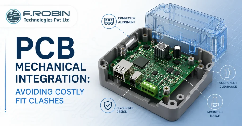
PCB mechanical integration is the practice of designing your board and its enclosure as one system, so they fit together perfectly the first time. When it goes well, connectors line up, components clear the lid, and assembly is effortless. When it goes wrong, you get fit clashes misaligned ports, components hitting the housing, mounting holes that miss and each one can trigger an expensive board or tooling respin. This guide explains how to get PCB mechanical integration right. We cover why fit clashes are so costly, what causes them, and the best practices that keep your board-to-enclosure design clash-free. Whether you build rugged industrial units or compact consumer devices, these techniques will save you time, money, and frustration. What Is PCB Mechanical Integration? PCB mechanical integration is the coordinated design of a printed circuit board and its mechanical enclosure so the two fit and function together. It ensures the board outline, components, connectors, and mounting points all align with the housing that surrounds them. In practice, this means the electrical and mechanical teams share information and a common 3D model throughout design. The board defines connector positions and component heights; the enclosure defines walls, cut-outs, and standoffs. PCB mechanical integration brings these two views together so nothing collides. Done well, it is invisible everything simply fits. Done poorly, it surfaces as clashes late in development, when fixes are most expensive. That is why treating board-to-enclosure design as one integrated task, not two separate ones, is the foundation of reliable hardware. Why Fit Clashes Are So Costly A single fit clash can be far more expensive than it first appears. Because mechanical and electrical issues often surface only after prototypes or tooling exist, fixing them means redoing expensive work. Poor PCB mechanical integration leads to costly outcomes: Each costs time and money that early integration would have prevented. The few hours spent coordinating board and enclosure up front save weeks of rework later — which is exactly why PCB mechanical integration deserves attention from day one. Common Causes of Fit Clashes Most fit problems trace back to a handful of recurring causes. Recognizing them early is half the battle. Almost all stem from designing the board and enclosure separately. When the two are integrated from the start, these clashes are caught on screen, not on the bench. PCB Mechanical Integration Best Practices Follow these best practices to keep board-to-enclosure design clash-free. Applied together, these practices turn PCB mechanical integration from a source of surprises into a predictable, repeatable process. They also tie directly into broader mechanical design services, where the enclosure and board evolve as one. The ECAD-MCAD Workflow The technical heart of PCB mechanical integration is exchanging data between electrical CAD (ECAD) and mechanical CAD (MCAD). The PCB tool holds the board and components; the MCAD tool — often SolidWorks — holds the enclosure. Keeping the two in sync is what prevents clashes. Teams typically share data using neutral formats: The goal is a single, shared source of truth. When the PCB moves a connector, the enclosure team sees it immediately; when the enclosure narrows a wall, the layout team adjusts. This continuous loop is what makes mechanical engineering and analysis of the assembly accurate and clash-free. Who Should Own the Integration? Fit clashes often slip through because no one clearly owns the board-and-enclosure handshake. The electrical team assumes the mechanical team is checking; the mechanical team assumes the opposite. Assigning one owner — or one shared review — closes that gap. On small teams, a single engineer comfortable in both ECAD and MCAD can own it. On larger projects, a brief integration review where both teams inspect the shared 3D assembly works well. Either way, make PCB mechanical integration a named responsibility with a checkpoint before release. When ownership is clear, clashes are caught early; when it is fuzzy, they reach the prototype bench — the most expensive place to find them. A Pre-Release Fit Checklist Before releasing the design, run through this quick checklist: Ticking every box before release is the simplest way to avoid a costly respin. If any item fails, fix it now — not after tooling. Common Mistakes to Avoid Even strong teams slip up on integration. Watch for these: Avoiding these keeps your PCB mechanical integration smooth and your project on schedule. Conclusion PCB mechanical integration is the difference between hardware that fits the first time and a project derailed by costly respins. By designing the board and enclosure as one system — sharing a 3D model, aligning connectors early, accounting for tolerance, and reviewing the full assembly before release — you eliminate the fit clashes that wreck schedules and budgets. Need Seamless PCB & Enclosure Integration? Avoid costly redesigns and mechanical fit issues. Our experts provide end-to-end Mechanical Engineering Services and PCB Layout Design Services to ensure your PCB, enclosure, and product architecture work together flawlessly from concept to production. Request a Design Consultation → Mechanical Engineering Services | PCB Layout Design Services Frequently Asked Questions 1. What is PCB mechanical integration? PCB mechanical integration is the coordinated design of a printed circuit board and its enclosure so they fit and function together, aligning the board outline, components, connectors, and mounting points with the housing. 2. Why is PCB mechanical integration important? It prevents costly fit clashes—misaligned connectors, components hitting the lid, or mismatched mounting holes—that would otherwise trigger board respins, tooling rework, and schedule delays. 3. What causes PCB-enclosure fit clashes? Common causes are connector misalignment, tall components, mismatched mounting holes, insufficient clearance, board outline errors, and tolerance stack-up—usually from designing the board and enclosure separately. 4. What is the ECAD-MCAD workflow? The ECAD-MCAD workflow exchanges data between electrical CAD (the PCB) and mechanical CAD (the enclosure, often in SolidWorks) using STEP and IDF/IDX formats, keeping both designs in sync. 5. How do I avoid connector alignment problems? Align connectors and ports with enclosure cut-outs early, share a common 3D model, and include tolerance margin so manufacturing variation does not cause
Custom PCB Design Services: When Off-the-Shelf Won’t Cut It
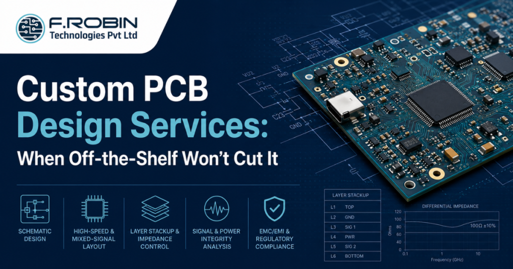
There is a moment in every hardware product cycle when a development module stops being a solution and starts being a constraint. The form factor is wrong. Unit costs are eroding margin. The RF noise is killing your analog front end. Your certification lab just handed back a failure report. That moment is when custom PCB design services become the only logical path forward. This guide helps hardware engineers, product managers, and procurement leads decide when to move from commercial modules to a purpose-built electronic PCB design — and what a professional engagement actually involves. What Are Custom PCB Design Services? Custom PCB design services are the end-to-end engineering process of designing a printed circuit board from the ground up — tailored to your product’s exact electrical, mechanical, thermal, and regulatory requirements. A professional PCB design company typically delivers: Custom electronic PCB design is not always necessary. But when it is, the gains in performance, size, cost, and certification compliance are difficult to achieve any other way. Off-the-Shelf vs. Custom PCB Design: Direct Comparison Factor Off-the-Shelf Module Custom PCB Design Time to Prototype Days to weeks 4–12 weeks NRE Cost None Moderate to high Unit Cost at Volume High (module premium) Low (optimized BOM) Form Factor Control Fixed Full control Regulatory Certification Often pre-certified Requires own testing IP Protection Low High proprietary design Mixed-Signal Performance Compromised Fully optimized Long-Term Supply Risk Module discontinuation Component-level sourcing Bottom line: For prototypes or low-volume internal tools, commercial modules are often the right call. For production-bound, certification-required, or cost-sensitive products, custom PCB design services pay for themselves. 7 Signs You Need Custom PCB Design Services 1. Your Form Factor Is Fixed and Modules Don’t Fit Medical wearables, aerospace enclosures, industrial handheld instruments — these have non-negotiable physical envelopes. When no commercial module fits, a custom PCB designed to exact mechanical constraints is the only option. 2. You’re Paying Module Premium at Production Volume Modules are priced for flexibility and small quantities. At 5,000+ units annually, the per-unit cost premium typically exceeds the original NRE investment within 12–18 months. 3. Your Design Has High-Speed Digital Signals Above 100 MHz — or with interfaces like DDR4, PCIe, USB 3.x, or MIPI — impedance-controlled routing and proper layer stackup are non-negotiable. These requirements demand high-speed digital and mixed-signal PCB layout expertise that commercial modules cannot substitute. 4. You’re Mixing Analog and Digital Domains Mixed-signal PCB design is among the most demanding disciplines in electronic PCB design. Poor ground plane management or insufficient isolation between analog and digital sections can destroy ADC performance or cause EMI failures. 5. Your Product Must Pass Regulatory Certification FCC Part 15, CE marking, IEC 60601 — certification evaluates the entire assembly. A PCB designed with EMC compliance in mind (shielding zones, controlled impedance, ferrite placement) has a significantly higher first-pass compliance rate. 6. You Have a Supply Chain or IP Concern Module vendors can discontinue products or become sole-source dependencies. Custom PCB design distributes sourcing risk across multiple suppliers and protects your architecture as proprietary IP. 7. Your Product Competes on Performance If your market position depends on a lower noise floor, faster processing, tighter latency, or higher precision, every compromised trace and shared power rail is a competitive liability. Custom PCB design services exist to remove these compromises. What Professional PCB Design Services Include Engaging a qualified PCB design company delivers more than a routed layout file. A full engagement covers: Schematic Capture and Review The design process starts with a verified schematic. The PCB design team reviews all reference designs, application notes, and datasheet recommendations. Errors caught here cost a fraction of what they cost after fabrication. Layer Stackup and Impedance Planning For high-speed or RF designs, the stackup is engineered before a single trace is routed. Layer count, dielectric material, copper weights, and layer assignments determine whether controlled impedance targets (50Ω single-ended, 100Ω differential) are achievable. Component Placement and Routing Experienced PCB designers apply thermal management, signal integrity, and DFM principles simultaneously during placement and routing. High-speed nets require length matching, guard routing, and verified return path continuity. DFM Review and Gerber Output A complete deliverable package includes fabrication-ready Gerber files, drill files, a BOM with approved alternates, assembly drawings, and a fabrication specification. High-Speed Digital and Mixed-Signal PCB Layout: Why It Matters High-speed digital and mixed-signal PCB layout combines signal integrity engineering, EMC design, and analog circuit principles — and is where most first-time custom PCB projects encounter problems. Key principles every PCB design company should apply: A poorly routed DDR5 interface can cause data corruption at speed. A shared ground between a switching regulator and a low-noise amplifier can inject hundreds of millivolts of noise into your signal chain. These are not edge cases — they’re common failure modes in designs that skip specialist mixed-signal PCB layout review. Key Takeaways Ready to Move from Module to Custom? If a commercial module is limiting your product’s performance, inflating costs, or blocking certification, it’s time to work with a PCB design team that understands the full engineering picture. Request a Design Consultation →
Talent Acquisition vs Recruitment: Are They the Same?
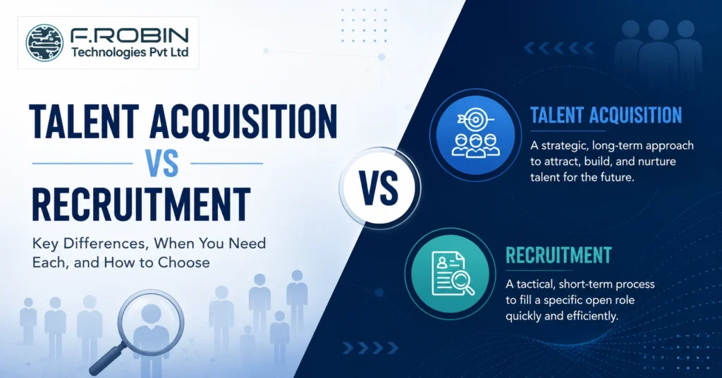
Talent acquisition and recruitment are often used interchangeably — but they are not the same thing. Recruitment is the tactical work of filling open roles, while talent acquisition is the broader, strategic approach to attracting and building talent over time. Confusing the two leads companies to hire reactively when they should be planning ahead. So are they the same? The short answer is no: recruitment is part of talent acquisition, not a synonym for it. In this comparison, we define each term, break down the key differences, and explain when you need one, the other, or both. By the end, you will know exactly which approach fits your hiring needs. What Is Talent Acquisition? Talent acquisition is the strategic, ongoing process of identifying, attracting, and building a pipeline of talent to meet a company’s long-term needs. Rather than reacting to a single vacancy, it plans ahead for the skills the business will need months or years from now. This strategic hiring approach includes workforce planning, employer branding, talent pipelines, and relationship-building with potential candidates. It treats hiring as a continuous investment, not a one-off event. As a result, companies with a strong talent strategy fill critical and senior roles faster, because they have already built relationships before the need arises. In short, it is about playing the long game ensuring the right people are available when the business needs them, especially for hard-to-fill technical and leadership roles. What Is Recruitment? Recruitment is the tactical process of filling a specific open role — sourcing, screening, interviewing, and hiring a candidate for a defined position. It starts when a vacancy opens and ends when the seat is filled. Recruitment is reactive by nature: a role becomes available, and the team moves to fill it quickly. It is essential, efficient, and the right tool for immediate hiring needs. Many companies use external recruitment services or a hiring agency to speed this up, especially for one-off or urgent roles. The key point is scope. Recruitment handles the here-and-now vacancy, while the wider strategy looks beyond it. Both matter, but they operate on different timelines and mindsets. Talent Acquisition vs Recruitment: The Key Differences The two differ across three core dimensions. Understanding these makes the distinction clear. Scope: Strategic vs Tactical It is strategic and ongoing, covering planning, branding, and pipeline building. Recruitment is tactical and specific, focused on filling the role in front of you. One is the long-term system; the other is a single transaction within it. Time Horizon: Long-Term vs Immediate A strategic approach plans for future skills needs, often months or years ahead. Recruitment addresses an immediate vacancy with a short, defined timeline. Therefore, the two answer different questions: “Who will we need?” versus “Who do we hire now?” Approach: Proactive vs Reactive It proactively nurtures relationships with potential candidates before roles open. Recruitment reacts once a role exists. Consequently, proactive pipelines shorten time-to-hire when a vacancy finally appears. Comparison Table The table below summarizes the two at a glance. Factor Talent Acquisition Recruitment Scope Strategic and ongoing Tactical and role-specific Time Horizon Long-term Immediate Approach Proactive Reactive Focus Building and nurturing a talent pipeline Filling a current vacancy Includes Employer branding, workforce planning, talent pipelines, and recruitment Sourcing, screening, interviewing, and hiring candidates Best For Critical, senior-level, and hard-to-fill positions Specific and immediate hiring requirements The clearest takeaway: recruitment is one activity inside the wider talent acquisition function. They are related, not identical. When You Need Talent Acquisition vs Recruitment Match the approach to your situation with these guidelines. Lean on recruitment when: Invest in talent acquisition when: In reality, most growing companies need both — fast recruitment for today’s openings and strategic hiring for tomorrow’s. The mix depends on your growth rate and the scarcity of your roles. How Talent Acquisition Works A strong function rests on a few connected pillars: These pillars feed each other. A strong employer brand fills the pipeline, the pipeline shortens time-to-hire, and good data sharpens planning. Together, they turn hiring from a scramble into a system. For specialized fields, this matters even more. In technology and engineering, the best candidates are rarely on the job market, so a proactive pipeline and employer brand are what win them. Do You Need Both? For most companies, the answer is yes. Recruitment handles immediate needs; a ready pipeline ensures you are never starting from zero when a critical role opens. Relying on recruitment alone keeps you in permanent catch-up mode, while strategy without execution never fills a seat. The smart approach blends them. Use a strategic approach to build pipelines and brand for your hardest roles, and efficient recruitment — often via a hiring agency or specialist partner to fill specific openings fast. Balanced together, they cut both cost and time-to-hire. This is especially true for fast-scaling firms, where today’s vacancy and next year’s skills gap both demand attention at once. Picture a fast-growing chip-design firm. It needs three verification engineers this quarter a clear recruitment job. At the same time, it knows it will need a design lead and ten more engineers within eighteen months. Building relationships with those future hires now, through an employer brand and a nurtured pipeline, is the strategic side. Handle only the urgent three and the firm will scramble later; handle both and it scales smoothly. Benefits of a Strong Hiring Strategy Investing beyond reactive hiring delivers lasting advantages: These gains compound. The longer you invest in this approach, the deeper your pipeline and the easier each future hire becomes. Common Misconceptions A few myths cloud this topic. Clearing them up helps you plan better: Avoiding these misconceptions keeps your hiring grounded in reality and your expectations realistic. Key Takeaways Conclusion Talent acquisition and recruitment are not the same. Recruitment fills today’s vacancy; it builds the pipeline and brand that make tomorrow’s hires faster and stronger. They differ in scope, time horizon, and approach — but they work best together. Most growing companies need efficient recruitment for immediate roles
Electronic Enclosure Design: Concept to Production
Mechanical enclosure design is the process of creating the protective housing that holds and shields your electronics from first sketch to production-ready tooling. A good enclosure does far more than look tidy: it protects the board, manages heat, resists the environment, and shapes how users interact with the product. Get it wrong, and you risk failures, rework, and costly tooling changes. This guide walks through electronic enclosure design from concept to production, stage by stage. You will learn how requirements turn into 3D CAD, how to choose materials, how tolerance and ingress protection shape the design, and how a concept becomes a manufacturable housing. Whether you are building a rugged industrial unit or a sleek consumer device, the path is the same. What Is Mechanical Enclosure Design? Mechanical enclosure design is the engineering of a physical housing that protects and packages electronic hardware. It covers the enclosure’s shape, material, fit, fastening, sealing, and thermal behaviour everything that keeps the electronics safe and usable. The discipline blends form and function. On one hand, the enclosure must protect the board from dust, moisture, shock, and heat. On the other, it must be manufacturable, serviceable, and pleasant to use. Because it touches mechanical, thermal, and industrial design at once, enclosure design is a true cross-disciplinary task. It also works hand in hand with the electronics inside. The board outline, connector positions, and mounting points all influence the housing, so good electronic enclosure design starts with the PCB and the enclosure considered together never in isolation. Why Mechanical Enclosure Design Matters A well-designed enclosure protects your investment and your users. Skimp on it, and even a brilliant board can fail in the field. Strong mechanical enclosure design delivers several benefits: The cost of getting it wrong is high. Late enclosure changes after tooling are slow and expensive, and a poor seal or weak mount can cause field returns. Therefore, investing in mechanical enclosure design early protects both reliability and budget. The Mechanical Enclosure Design Process: Concept to Production Here is how concept-to-production design unfolds, stage by stage. Each step builds on the last. Step 1: Requirements and Specification Start by capturing requirements: size limits, environment, IP rating, thermal load, mounting, ports, certifications, and volume. A clear spec anchors every later decision and prevents costly surprises. Step 2: Concept Design Next, explore concepts. Sketches and rough 3D models test different forms, layouts, and split lines. This is the cheapest stage to experiment, so explore several directions before committing. Step 3: Detailed 3D CAD Now build the detailed model. Engineers create the enclosure in 3D CAD commonly SolidWorks defining walls, bosses, ribs, and features precisely. The PCB model is imported so the housing fits the board exactly. Step 4: Material Selection With the form set, choose the material. Material selection balances strength, cost, weight, thermal needs, and looks. We cover the main options below. Step 5: Tolerance and DFM Then refine for manufacturing. Tolerance analysis ensures parts fit reliably, while design for manufacturability (DFM) tunes features for the chosen process moulding, sheet metal, or machining. Step 6: Prototyping and Validation Build prototypes — often 3D printed or machined — and test fit, function, thermal, and ingress. Validation here catches issues while changes are still cheap, before tooling. Step 7: Production and Tooling Finally, commit to production. Tooling (such as injection moulds) is cut, first articles are inspected, and volume manufacturing begins. A clean handoff here turns your design into real, repeatable parts. Material Selection for Enclosures Material drives cost, durability, and process. The table compares common enclosure materials. Material Strengths Best For Injection-moulded Plastic Low unit cost at volume, excellent design freedom Consumer and high-volume products Sheet Metal Strong, good for shielding, low tooling cost Industrial and low-to-mid volume products Die-cast Aluminium Rugged, excellent thermal and EMI shielding Rugged, high-reliability units Aluminium Extrusion Cost-effective for long, simple shapes Rack units, amplifiers, and instruments There is no single best material — the right choice depends on volume, environment, and budget. For high-power products, thermal performance often drives the decision; for consumer goods, cost and finish lead. Ingress Protection (IP Ratings) Ingress protection defines how well an enclosure keeps out dust and water, expressed as an IP rating (for example, IP65). The first digit rates solids, the second rates liquids. Choosing the right rating early shapes seals, gaskets, and joints throughout the design. Common targets include: Over-specifying ingress protection adds cost and complexity, while under-specifying risks failure. Match the IP rating to the real operating environment, and design seals and gaskets to achieve it from the start — retrofitting sealing later is difficult and unreliable. Tolerance and Fit Tolerance is where good mechanical enclosure design succeeds or fails. Parts must fit together, align with the PCB, and accommodate manufacturing variation all at once. Loose tolerances cause rattles and gaps; overly tight tolerances raise cost without benefit. A tolerance stack-up analysis checks that the accumulated variation across mating parts still produces a reliable fit. It is especially important where the enclosure meets connectors, buttons, and the board, since misalignment here is highly visible to users. The goal is balance: specify tolerances tight enough to work, but loose enough to manufacture affordably. Coordinating closely with the PCB through solid PCB layout design services — keeps connector and mount positions aligned with the housing. Mechanical Enclosure Design and the PCB The single biggest predictor of enclosure success is how early it is coordinated with the board. Mechanical enclosure design and PCB layout should advance together, sharing the same 3D model so connectors, mounting holes, and tall components never clash with the housing. When the two teams work in sync, problems surface on screen instead of on the bench. Connector cut-outs line up, standoffs land on real pads, and tall capacitors clear the lid. When they work in isolation, the first prototype reveals expensive surprises. A shared 3D CAD workflow exporting the PCB into the enclosure model turns mechanical enclosure design from a guessing game into a precise, predictable process. This
Recruitment Services Explained: Permanent, Contract & RPO
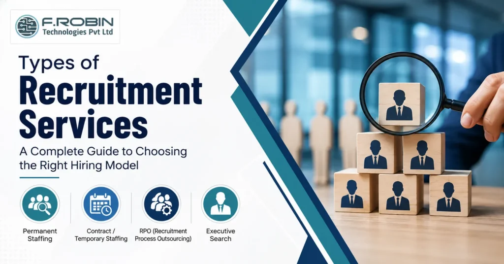
Recruitment services help companies find, attract, and hire the right people without carrying the full burden of hiring alone. But “recruitment services” is an umbrella term that covers very different models — permanent staffing, contract staffing, RPO, and executive search — each suited to a different hiring need. Choosing the wrong one wastes time and money; choosing the right one fills critical roles fast. This guide explains the main types in plain language and shows when to use each. Whether you are hiring one engineer, scaling a whole team, or filling a leadership seat, understanding these options helps you partner smartly and hire with confidence. What Are Recruitment Services? Recruitment services are professional hiring solutions that source, screen, and place candidates on behalf of an employer. In short, a provider handles part or all of your hiring process so you can fill roles faster and with less effort. These services range from filling a single permanent role to managing an entire hiring function. Some providers focus on speed and volume; others specialize in scarce skills or senior leadership. The best fit depends on your role type, timeline, and how much of the process you want to outsource. For technology and engineering teams especially, specialist providers bring deep talent networks that an internal team rarely matches. That access is often the difference between a six-week hire and a six-month one. The Main Types of Recruitment Services Most providers offer several models. Here are the four you will encounter most often. Permanent Staffing Permanent staffing fills full-time, long-term roles. The provider sources and screens candidates, and you hire the chosen person directly onto your payroll. This model suits core roles you intend to keep, and it is the most common form of hiring service. Contract / Temporary Staffing Contract staffing places workers for a fixed period or specific project. The staffing firm often employs the worker, handling payroll and compliance, while they work under your direction. This model gives you flexibility to scale up and down without long-term commitment. RPO (Recruitment Process Outsourcing) RPO means outsourcing all or part of your recruitment function to a provider who runs it as an extension of your team. RPO suits high-volume or ongoing hiring, delivering process, technology, and scale. As a result, it lowers cost-per-hire and improves consistency. Executive Search Executive search — also called headhunting — finds senior leaders and hard-to-fill specialists. It is a focused, often retained service that proactively approaches passive candidates. Use it for critical leadership roles where the right hire transforms the business. Recruitment Services Compared The table below compares the four main types at a glance. Model Best For Engagement Typical Cost Model Permanent Staffing Core, long-term roles Per placement Percentage of annual salary Contract Staffing Projects and flexible scaling Fixed term Hourly or monthly markup RPO (Recruitment Process Outsourcing) High-volume, ongoing hiring Long-term partnership Monthly fee or per-hire fee Executive Search Senior and hard-to-find leadership roles Retained search Retainer plus success fee Reading across the rows shows there is no single “best” model only the best fit for a given hiring need. Many companies blend several, using permanent staffing for core roles and contract or RPO for surges. When to Use Each Type Match the model to your situation with these guidelines. In practice, your needs may span more than one model. A growing technology firm, for example, might use permanent staffing for engineers, contract staffing for a project spike, and executive search for a new head of engineering all at once. How Recruitment Services Work Whatever the model, good providers follow a clear process: This structure reduces your time-to-hire and protects candidate experience. Consequently, a strong process is one of the clearest signs of a capable partner. Benefits of Using a Recruitment Partner Partnering with a provider delivers real advantages: These benefits compound on hard-to-fill roles, where the cost of a vacancy or a bad hire far outweighs the cost of expert help. In technology hiring especially, where a single unfilled senior role can stall a product roadmap, that speed and reach translate directly into shipped products and protected revenue. In-House Hiring vs Using a Provider Should you hire through your own team or bring in a provider? In-house hiring gives you full control and deep cultural knowledge, but it depends on your recruiters’ bandwidth and reach. When roles are scarce, urgent, or high-volume, an internal team can quickly hit its limits. A provider adds reach, speed, and specialist networks on demand. For a steady trickle of common roles, in-house often works well. For surges, niche skills, or leadership hires, outside help usually pays for itself. Many companies run a hybrid model — keeping everyday hiring in-house and calling in a partner for the hard roles. The cost comparison matters too. Internal recruiting carries fixed salary and tooling costs regardless of output, while a provider’s fee scales with actual hiring. For variable or seasonal demand, that flexibility is often the deciding factor. How to Choose the Right Recruitment Services Partner Not every provider fits every need. Evaluate candidates on a few key points: If your hiring centres on engineering, semiconductor, EMS, or AI talent, a specialist partner like our AI staffing services brings the domain networks and screening depth those roles demand. You can also review our client outcomes to gauge fit. Key Takeaways Conclusion Recruitment services come in four main forms permanent staffing, contract staffing, RPO, and executive search and the right choice depends on your role, timeline, and volume. Permanent suits core hires, contract gives flexibility, RPO scales high-volume hiring, and executive search secures critical leaders. Many companies use several together, and the best partners offer all of them. Need Specialized Talent? Hiring for Technology, Semiconductor, EMS, or AI roles? Our AI staffing services combine deep domain expertise with Permanent Staffing, Contract Staffing, and RPO solutions to help you find the right talent faster. Whether you’re scaling a team, filling niche positions, or managing high-volume hiring, our specialists can build a hiring strategy tailored
HR Consulting: When Should You Bring in an Expert?

HR consulting brings outside expertise to solve people problems your internal team cannot tackle alone. From compliance gaps and high turnover to messy restructures, the right expert can fix issues fast — and prevent costly mistakes. But how do you know when to bring one in versus handling things yourself? This decision guide lays out the clear signs you need expert support, what consultants actually do, and when in-house HR is enough on its own. Whether you are a fast-growing startup or an established firm facing change, these signals will help you decide with confidence rather than waiting until a small problem becomes an expensive one. What Is HR Consulting? HR consulting is a professional service that provides expert advice and hands-on support across human resources — from strategy and compliance to org design and culture. In short, an HR consultant diagnoses people problems and helps you solve them, either as a one-off project or an ongoing partnership. Unlike day-to-day HR administration, this work is strategic and specialized. A consultant brings cross-industry experience, current best practice, and an objective outside view that internal teams often lack. As a result, companies turn to outside experts when the stakes are high or the problem sits outside their in-house expertise. The scope is broad. It can cover HR strategy, policy, compensation, performance management, restructuring, and compliance whatever the business needs at that moment. Signs You Need HR Consulting Support How do you know it is time to call an expert? Watch for these clear signals. If several of these ring true, expert help is worth serious consideration. The cost of expert help is almost always lower than the cost of a compliance penalty, a wrongful-termination claim, or a wave of regretted hires. What HR Consultants Actually Do HR consultants cover far more than hiring advice. Their work typically spans several areas: Many providers also connect this work with broader workforce solutions, so strategy, hiring, and talent management work together rather than in silos. That joined-up approach is often where the biggest gains come from. HR Consulting vs In-House HR vs Recruitment These functions overlap but solve different problems. The table clarifies the difference. Service Focus Best for HR Consulting Strategy, policy, compliance, and organizational change Complex or one-off people challenges In-House HR Day-to-day people operations Ongoing administration and employee support Recruitment / Staffing Sourcing and placing candidates Filling specific roles quickly and effectively In practice, the three complement each other. A consulting firm sets strategy and policy, in-house HR runs daily operations, and recruitment services fill the roles. Knowing which you need — or which combination — saves time and money. When You Don’t Need HR Consulting An expert is not always the answer. You can likely skip outside help when: Bringing in a consultant for purely routine work wastes budget. The value appears when the problem is complex, high-risk, or beyond your team’s current capability — not for everyday tasks an internal team handles well. Benefits of HR Consulting When the fit is right, the advantages are significant: These benefits matter most during change or growth, when a single misstep a botched restructure or a compliance breach can cost far more than the engagement itself. Crucially, good consultants also transfer knowledge. A strong engagement upskills your managers and HR staff, so the improvements outlast the project itself — turning a one-time fix into a lasting internal capability. How HR Consulting Engagements Work Engagements come in a few common shapes, and the right one depends on your need: Most engagements start with a discovery phase: the consultant audits your current people practices, identifies gaps and risks, and proposes a prioritized plan. From there, they either deliver the work directly or coach your team to do it. Either way, agree how you will measure success — fewer compliance gaps, lower turnover, a faster hiring process — so the value is visible. A good consultant leaves your team stronger, not dependent. How to Choose an HR Consulting Partner Not every provider suits every need. Evaluate candidates on these points: For technology and engineering firms scaling teams, a partner who pairs people strategy with hiring expertise is especially valuable. Our AI staffing services connect people strategy with specialist recruitment, and our client outcomes show how that combination works in practice. Key Takeaways Conclusion HR consulting is worth bringing in when people challenges grow complex, risky, or beyond your team’s expertise rapid growth, compliance gaps, high turnover, restructures, or major change. For routine work in a small, stable team, your in-house resources are usually enough. The key is recognizing the signals early, before a manageable issue becomes an expensive one. Need HR Strategy and Specialist Hiring Support? Scaling a Technology, Semiconductor, EMS, or AI team and need both people strategy and specialist recruitment expertise? Our AI staffing services combine HR consulting, workforce planning, and domain-focused hiring solutions to help you build and grow high-performing teams. Whether you’re expanding rapidly or filling critical positions, we can provide the right support for your stage. Talk to Our Team Frequently Asked Questions 1. What is HR consulting? HR consulting is a professional service that provides expert advice and hands-on support across human resources, including HR strategy, policy, organizational design, compensation, and compliance. It can be delivered as a one-time project or an ongoing partnership. 2. When should I bring in an HR consultant? Consider bringing in an HR consultant during periods of rapid growth, compliance uncertainty, high employee turnover, restructuring, outdated policies, or major organizational change such as a merger or acquisition. Expert guidance can help reduce risk and improve outcomes. 3. What does an HR consultant do? An HR consultant identifies people-related challenges and helps solve them through HR strategy, policy development, employee handbooks, organizational design, compliance support, compensation and benefits planning, performance management, and change management initiatives. 4. What is the difference between HR consulting and in-house HR? HR consulting provides strategic and specialized expertise for complex or one-off challenges, while in-house HR teams manage daily people
PCB Mechanical Integration: Avoiding Costly Fit Clashes
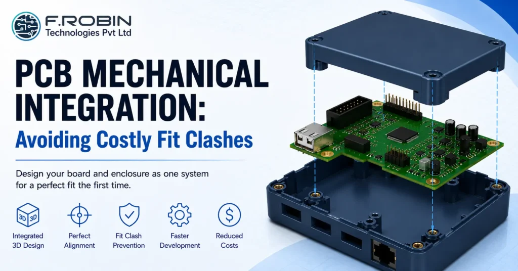
PCB mechanical integration is the practice of designing your board and its enclosure as one system, so they fit together perfectly the first time. When it goes well, connectors line up, components clear the lid, and assembly is effortless. When it goes wrong, you get fit clashes misaligned ports, components hitting the housing, mounting holes that miss and each one can trigger an expensive board or tooling respin. This guide explains how to get PCB mechanical integration right. We cover why fit clashes are so costly, what causes them, and the best practices that keep your board-to-enclosure design clash-free. Whether you build rugged industrial units or compact consumer devices, these techniques will save you time, money, and frustration. What Is PCB Mechanical Integration? PCB mechanical integration is the coordinated design of a printed circuit board and its mechanical enclosure so the two fit and function together. It ensures the board outline, components, connectors, and mounting points all align with the housing that surrounds them. In practice, this means the electrical and mechanical teams share information and a common 3D model throughout design. The board defines connector positions and component heights; the enclosure defines walls, cut-outs, and standoffs. PCB mechanical integration brings these two views together so nothing collides. Done well, it is invisible — everything simply fits. Done poorly, it surfaces as clashes late in development, when fixes are most expensive. That is why treating board-to-enclosure design as one integrated task, not two separate ones, is the foundation of reliable hardware. Why Fit Clashes Are So Costly A single fit clash can be far more expensive than it first appears. Because mechanical and electrical issues often surface only after prototypes or tooling exist, fixing them means redoing expensive work. Poor PCB mechanical integration leads to costly outcomes: Each of these costs time and money that early integration would have prevented. In short, the few hours spent coordinating board and enclosure up front save weeks of rework later which is exactly why PCB mechanical integration deserves attention from day one. Common Causes of Fit Clashes Most fit problems trace back to a handful of recurring causes. Recognizing them early is half the battle. Almost all of these stem from designing the board and enclosure separately. When the two are integrated from the start, these clashes are caught on screen instead of on the bench. PCB Mechanical Integration Best Practices Follow these best practices to keep board-to-enclosure design clash-free. Applied together, these practices turn PCB mechanical integration from a source of surprises into a predictable, repeatable process. They also tie directly into broader mechanical design services, where the enclosure and board evolve as one. The ECAD-MCAD Workflow The technical heart of PCB mechanical integration is exchanging data between electrical CAD (ECAD) and mechanical CAD (MCAD). The PCB tool holds the board and components; the MCAD tool — often SolidWorks — holds the enclosure. Keeping them in sync is what prevents clashes. Teams typically share data using neutral formats: The goal is a single, shared source of truth. When the PCB moves a connector, the enclosure team sees it immediately; when the enclosure narrows a wall, the layout team adjusts. This continuous loop is what makes mechanical engineering and analysis of the assembly accurate and clash-free. A Pre-Release Fit Checklist Before releasing the design, run through this quick checklist: Ticking every box before release is the simplest way to avoid a costly respin. If any item fails, fix it now not after tooling. Common Mistakes to Avoid Even strong teams slip up on integration. Watch for these: Avoiding these keeps your PCB mechanical integration smooth and your project on schedule. Key Takeaways Conclusion PCB mechanical integration is the difference between hardware that fits the first time and a project derailed by costly respins. By designing the board and enclosure as one system — sharing a 3D model, aligning connectors early, accounting for tolerance, and reviewing the full assembly before release — you eliminate the fit clashes that wreck schedules and budgets. Building a Product Where the PCB and Enclosure Must Fit Perfectly? Our mechanical engineering services and PCB layout design services handle PCB mechanical integration from concept to production. Work with our engineering team to eliminate design clashes, reduce development risk, and accelerate time to market. Talk to Our Engineering Team Frequently Asked Questions 1. What is PCB mechanical integration? PCB mechanical integration is the coordinated design of a printed circuit board and its enclosure so they fit and function together, aligning the board outline, components, connectors, and mounting points with the housing. 2. Why is PCB mechanical integration important? It prevents costly fit clashes — misaligned connectors, components hitting the lid, or mismatched mounting holes — that would otherwise trigger board respins, tooling rework, and schedule delays. 3. What causes PCB-enclosure fit clashes? Common causes are connector misalignment, tall components, mismatched mounting holes, insufficient clearance, board outline errors, and tolerance stack-up — usually from designing board and enclosure separately. 4. What is the ECAD-MCAD workflow? The ECAD-MCAD workflow exchanges data between electrical CAD (the PCB) and mechanical CAD (the enclosure, often in SolidWorks) using STEP and IDF/IDX formats, keeping both designs in sync. 5. How do I avoid connector alignment problems? Align connectors and ports with enclosure cut-outs early, share a common 3D model, and include tolerance margin so manufacturing variation does not cause misalignment. “`
PCB Manufacturing: A Complete Guide From Gerbers to Boards
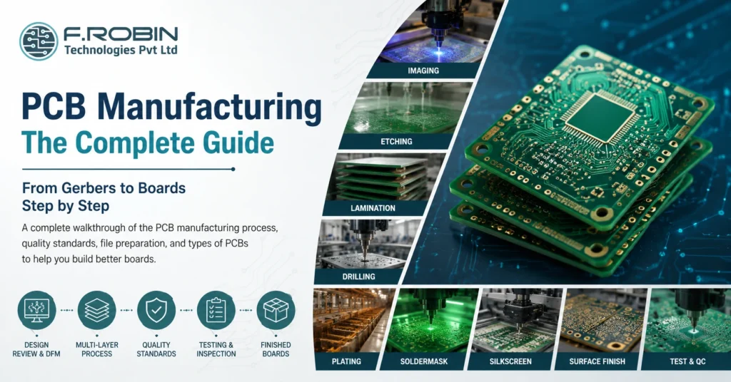
PCB manufacturing is the process of turning your design files into physical, ready-to-assemble circuit boards. It begins with Gerber data and ends with finished, tested boards — passing through imaging, etching, lamination, drilling, plating, and more along the way. If you have ever wondered what happens between hitting “export” and holding your board, this guide walks you through every stage. Understanding the process helps you design better boards, control cost, and choose the right partner. Whether you are comparing printed circuit board manufacturers or simply curious how circuit board manufacturing works, this complete guide takes you from Gerbers to boards, step by step. What Is PCB Manufacturing? PCB manufacturing, also called PCB fabrication, is the process of building a bare printed circuit board from design data. It transforms copper-clad laminate into a board with precise traces, layers, holes, and finishes, ready to receive components. The process is highly automated and tightly controlled, because tiny errors at this scale cause real failures. Most printed circuit board manufacturers follow IPC standards to guarantee consistent quality across every batch. As a result, a well-made board behaves exactly as the designer intended. It helps to remember what this stage does and does not include. Fabrication produces the empty board; it does not add components. That second step is assembly, which we cover in our guide to PCB assembly. Together, fabrication and assembly deliver a finished, working product. PCB Manufacturing vs PCB Assembly People often confuse these two stages, so let us be clear. Circuit board manufacturing creates the bare board — copper, layers, holes, soldermask, and finish. Assembly then solders components onto that board. In short: manufacturing makes the board; assembly populates it. Some vendors offer both as a turnkey service, while others specialize in one. Knowing the difference helps you scope quotes accurately and avoid surprises in your timeline. The PCB Manufacturing Process Step by Step Here is how pcb manufacturing turns Gerber files into finished boards. While details vary by factory, the core flow is consistent. Step 1: Design Review and DFM First, the factory reviews your Gerber or ODB++ files and runs a design-for-manufacturability (DFM) check. This catches issues like undersized traces or tight clearances before any material is cut. Step 2: Inner Layer Imaging and Etching Next, the inner copper layers are imaged with the circuit pattern. Etching then removes unwanted copper, leaving only the traces you designed. Precision here defines your final trace widths and impedance. Step 3: Lamination The etched inner layers are stacked with prepreg and copper foil, then bonded under heat and pressure. This lamination step fuses the layers into a single solid board — the heart of multilayer construction. Step 4: Drilling Now machines drill the holes for vias and through-hole parts. Modern drilling uses CNC and, for the smallest holes, lasers. Accurate drilling is essential for reliable connections between layers. Step 5: Plating and Through-Hole Metallization Copper plating coats the drilled holes, electrically connecting layers. This through-hole metallization is what turns a stack of separate layers into one connected circuit. Step 6: Outer Layer Imaging and Etching The outer layers are then imaged and etched, just like the inner layers, to form the surface traces and pads. Step 7: Soldermask and Silkscreen A soldermask is applied to protect the copper and prevent solder bridges, giving the board its familiar color. A silkscreen legend adds reference designators, logos, and markings. Step 8: Surface Finish A surface finish — such as ENIG, HASL protects exposed pads and ensures solderability during assembly. Step 9: Electrical Test and Final QC Finally, the boards are electrically tested for opens and shorts, inspected against IPC standards, then routed to their final shape and shipped. Clean files at the start make this final stage fast and trouble-free. Types of PCBs You Can Manufacture Pcb manufacturing supports many board types. The table below summarizes the main options. Type Description Typical Use Rigid 30 Layer Most products Multilayer Three or more layers Dense, high-speed designs Flexible 6 Layers Wearables, tight spaces Rigid-Flex 24 Layer Compact, reliable assemblies HDI High-density interconnect Fine-pitch, miniaturized boards Metal-Core Aluminum or copper base High-power, LED, and thermal-heavy applications Choosing the right type early shapes your cost and capability. For multilayer choices specifically, see our guide on multilayer PCB design. PCB Manufacturing Quality Standards Quality is not optional in circuit board manufacturing. Reputable printed circuit board manufacturers work to recognized standards: Asking which IPC class and certifications a supplier holds is a fast way to judge their quality discipline. A capable partner will state these clearly and back them with inspection reports. How to Prepare Your Files for PCB Manufacturing Clean data makes pcb manufacturing smooth and fast. Before you order, prepare a complete package: These outputs flow directly from your layout. For the upstream steps, see our printed circuit board design workflow guide, and finalize your data with professional PCB layout design services. How to Reduce PCB Manufacturing Cost You can lower cost without hurting quality by designing smartly. Try these proven tactics: Small design choices add up. Consequently, working with your manufacturer early often saves more than any single tactic on its own. Common PCB Manufacturing Mistakes to Avoid Watch for these frequent pitfalls: Avoiding these mistakes keeps your boards reliable, on budget, and on schedule. How to Choose a PCB Manufacturer Picking the right fab is as important as the design itself. Look beyond the headline price and weigh a few key factors: Think about your stage, too. For early prototypes, fast turnaround and flexibility matter most. For production, consistency, yield, and cost per board take over. Many teams start with a quick-turn shop for prototypes, then qualify a volume partner — or choose one fab that does both well to avoid re-qualifying later. For demanding products, prioritize quality discipline and engineering support over the lowest quote, because a respin almost always costs more than the savings. Key Takeaways Conclusion PCB manufacturing follows a clear, repeatable journey from Gerber files to finished boards: review and
Circuit Board Manufacturing: Prototype vs Production
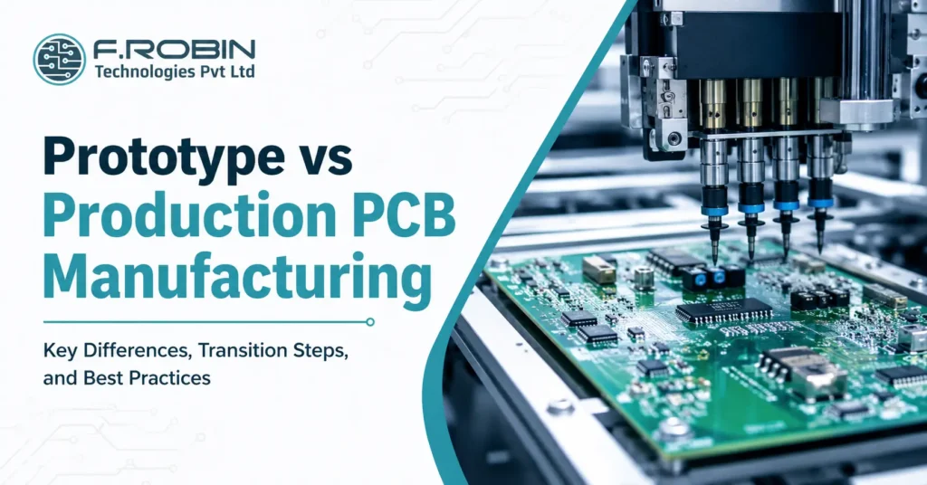
Circuit board manufacturing looks very different at the prototype stage than it does in full production. A prototype proves your design works; production proves you can build it reliably, affordably, and at scale. Confuse the two and you risk wasted money, delays, or a board that works in the lab but stumbles on the line. So what actually changes as you move from a handful of boards to thousands? In this guide, we compare prototype and production circuit board manufacturing across cost, lead time, testing, tooling, and yield. You will also learn how to transition smoothly between the two — and the mistakes that trip teams up when they scale. What Changes Between Prototype and Production? The short answer: the goal changes. Prototype circuit board manufacturing optimizes for speed and learning, while production optimizes for cost, consistency, and yield. As a result, almost every choice from quantity to testing shifts when you scale your circuit board manufacturing. In the prototype phase, you build a few boards quickly to validate the design. Mistakes are expected, and revisions are frequent. By contrast, production assumes the design is locked. Here the focus moves to repeatable quality, low cost per board, and high yield across thousands of units. Understanding this shift early saves money. A board designed only to “work once” rarely survives the demands of mass production, so smart teams plan for both stages from the start. For the underlying process itself, see our PCB manufacturing guide. This stage shift also changes who you talk to and what you measure. In prototyping, engineers chase functionality and iterate fast. In production circuit board manufacturing, operations and quality teams chase repeatability, tracking yield, defect rates, and cost per board on every run. Recognizing that the metrics themselves change helps you set the right expectations with your manufacturer at each stage. Prototype Circuit Board Manufacturing The prototype stage exists to answer one question: does the design work? Speed and flexibility matter most here, not cost per board. Typical traits of prototype circuit board production include: Because you are still learning, prototypes prioritize fast feedback over efficiency. The aim is to find and fix problems cheaply, before they multiply across thousands of units. The Pilot / Pre-Production Run Between prototype and full production sits the pilot run a small batch, often 50 to a few hundred boards, built on production-like processes. This bridge stage is easy to skip but valuable to keep. A pilot run verifies that your design is ready for volume. It exposes assembly issues, confirms test coverage, and reveals yield problems before you commit to a large order. Consequently, a good pilot prevents expensive surprises during mass production. Think of it as a dress rehearsal for the production line. So when are you ready to scale? You are ready when the design is stable across several prototypes, the pilot hits an acceptable yield, and your test coverage reliably catches real defects. Until those three boxes are ticked, moving to volume circuit board manufacturing only multiplies risk. Production Circuit Board Manufacturing Production circuit board manufacturing assumes the design is final and shifts the focus to scale. Now cost, consistency, and yield drive every circuit board manufacturing decision. Typical traits of production-stage printed circuit board production include: At this stage, small inefficiencies multiply. Therefore, production rewards careful design-for-manufacturing (DFM) and disciplined process control far more than the prototype stage ever did. Getting DFM right before this point is the single best lever for protecting yield at volume. Prototype vs Production: Side-by-Side This table summarizes how circuit board manufacturing changes across the two stages. Factor Prototype PCB Manufacturing Production PCB Manufacturing Quantity 1–50 boards Hundreds to thousands of boards Cost per Board High High Lead Time week Longer setup, fast throughput Automation Low priority Full automation Revisions Frequent design changes Design locked and validated Testing Basic and functional testing ICT, AOI, and comprehensive functional testing Yield Focus High priority priority Critical manufacturing metric Goal Validate the design Scale production reliably and cost-effectively Use this as a planning reference. The clearer you are about which stage you are in, the better your quotes and timelines will be. How to Transition From Prototype to Production Scaling up your circuit board manufacturing is a process, not a single leap. Follow these steps for a smooth transition: This staged approach reduces risk at every step. Moreover, qualifying your fab and assembly partner early ideally one that also offers PCB assembly avoids re-qualification later. Choosing the Right Partner for Each Stage Not every fab excels at both stages of circuit board manufacturing. Quick-turn shops shine at prototypes but may lack volume capacity, while large-volume houses can be slow and costly for a handful of boards. So match the partner to your stage — or choose one that does both well. For prototypes, prioritize speed, flexibility, and responsive support. For production, prioritize capacity, yield discipline, and competitive cost per board. A partner that handles prototype, pilot, and production circuit board manufacturing under one roof saves you from re-qualifying a new supplier mid-project, which protects both your timeline and your hard-won yield data. If you expect to scale, raise the question early. Ask prospective suppliers how they handle the jump from prototype to pcb board production, what their typical yields are at volume, and how they manage the pilot stage in between. Their answers quickly reveal whether they can grow with you. Common Mistakes When Scaling Up Teams often stumble at the prototype-to-production handoff. Watch for these: Avoiding these mistakes keeps your circuit board production reliable, profitable, and on schedule. Key Takeaways Conclusion Circuit board manufacturing is not one process but two mindsets. Prototyping chases speed and learning; production chases cost, consistency, and yield. The teams that scale smoothly plan for both from day one — locking the design, running a pilot, tightening test coverage, and qualifying their supplier before ramping volume. Ready to Take Your Board from Prototype to Production? Our PCB manufacturing services support everything from quick-turn prototypes to high-volume production
