
PCB manufacturing is the process of turning your design files into physical, ready-to-assemble circuit boards. It begins with Gerber data and ends with finished, tested boards — passing through imaging, etching, lamination, drilling, plating, and more along the way. If you have ever wondered what happens between hitting “export” and holding your board, this guide walks you through every stage.
Understanding the process helps you design better boards, control cost, and choose the right partner. Whether you are comparing printed circuit board manufacturers or simply curious how circuit board manufacturing works, this complete guide takes you from Gerbers to boards, step by step.
What Is PCB Manufacturing?
PCB manufacturing, also called PCB fabrication, is the process of building a bare printed circuit board from design data. It transforms copper-clad laminate into a board with precise traces, layers, holes, and finishes, ready to receive components.
The process is highly automated and tightly controlled, because tiny errors at this scale cause real failures. Most printed circuit board manufacturers follow IPC standards to guarantee consistent quality across every batch. As a result, a well-made board behaves exactly as the designer intended.
It helps to remember what this stage does and does not include. Fabrication produces the empty board; it does not add components. That second step is assembly, which we cover in our guide to PCB assembly. Together, fabrication and assembly deliver a finished, working product.
PCB Manufacturing vs PCB Assembly
People often confuse these two stages, so let us be clear. Circuit board manufacturing creates the bare board — copper, layers, holes, soldermask, and finish. Assembly then solders components onto that board.
In short: manufacturing makes the board; assembly populates it. Some vendors offer both as a turnkey service, while others specialize in one. Knowing the difference helps you scope quotes accurately and avoid surprises in your timeline.
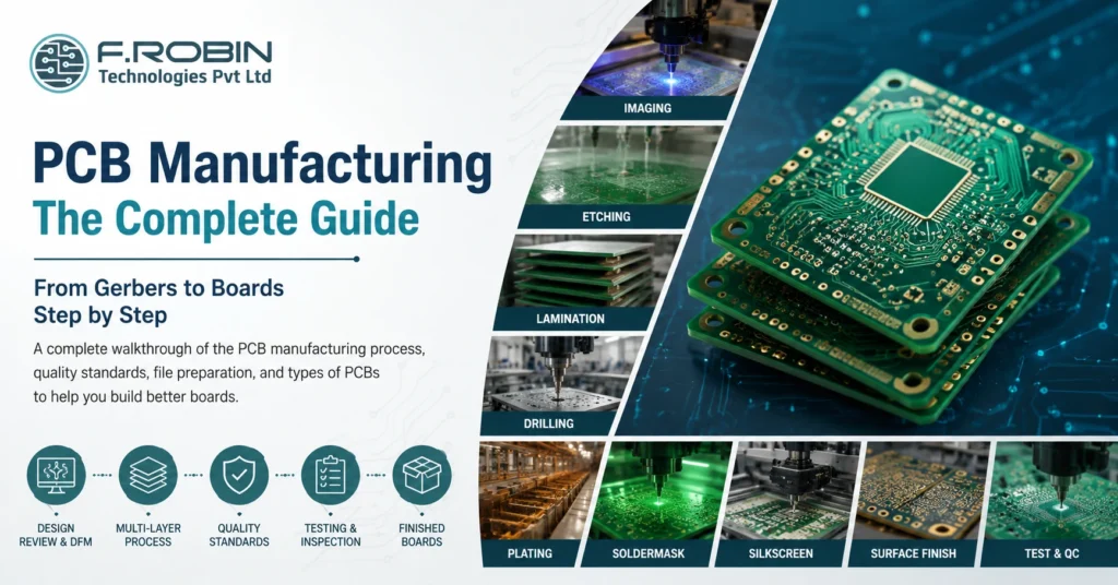
The PCB Manufacturing Process Step by Step
Here is how pcb manufacturing turns Gerber files into finished boards. While details vary by factory, the core flow is consistent.
Step 1: Design Review and DFM
First, the factory reviews your Gerber or ODB++ files and runs a design-for-manufacturability (DFM) check. This catches issues like undersized traces or tight clearances before any material is cut.
Step 2: Inner Layer Imaging and Etching
Next, the inner copper layers are imaged with the circuit pattern. Etching then removes unwanted copper, leaving only the traces you designed. Precision here defines your final trace widths and impedance.
Step 3: Lamination
The etched inner layers are stacked with prepreg and copper foil, then bonded under heat and pressure. This lamination step fuses the layers into a single solid board — the heart of multilayer construction.
Step 4: Drilling
Now machines drill the holes for vias and through-hole parts. Modern drilling uses CNC and, for the smallest holes, lasers. Accurate drilling is essential for reliable connections between layers.
Step 5: Plating and Through-Hole Metallization
Copper plating coats the drilled holes, electrically connecting layers. This through-hole metallization is what turns a stack of separate layers into one connected circuit.
Step 6: Outer Layer Imaging and Etching
The outer layers are then imaged and etched, just like the inner layers, to form the surface traces and pads.
Step 7: Soldermask and Silkscreen
A soldermask is applied to protect the copper and prevent solder bridges, giving the board its familiar color. A silkscreen legend adds reference designators, logos, and markings.
Step 8: Surface Finish
A surface finish — such as ENIG, HASL protects exposed pads and ensures solderability during assembly.
Step 9: Electrical Test and Final QC
Finally, the boards are electrically tested for opens and shorts, inspected against IPC standards, then routed to their final shape and shipped. Clean files at the start make this final stage fast and trouble-free.
Types of PCBs You Can Manufacture
Pcb manufacturing supports many board types. The table below summarizes the main options.
| Type | Description | Typical Use |
|---|---|---|
| Rigid | 30 Layer | Most products |
| Multilayer | Three or more layers | Dense, high-speed designs |
| Flexible | 6 Layers | Wearables, tight spaces |
| Rigid-Flex | 24 Layer | Compact, reliable assemblies |
| HDI | High-density interconnect | Fine-pitch, miniaturized boards |
| Metal-Core | Aluminum or copper base | High-power, LED, and thermal-heavy applications |
Choosing the right type early shapes your cost and capability. For multilayer choices specifically, see our guide on multilayer PCB design.
PCB Manufacturing Quality Standards
Quality is not optional in circuit board manufacturing. Reputable printed circuit board manufacturers work to recognized standards:
- IPC Class 2 — general electronics, the most common class.
- IPC Class 3 — high-reliability products like medical, aerospace, and defence.
- IPC-A-600 — defines the acceptability of bare boards.
- UL certification — safety marking required for many products.
- RoHS / REACH — environmental compliance for materials.
Asking which IPC class and certifications a supplier holds is a fast way to judge their quality discipline. A capable partner will state these clearly and back them with inspection reports.
How to Prepare Your Files for PCB Manufacturing
Clean data makes pcb manufacturing smooth and fast. Before you order, prepare a complete package:
- Gerber (RS-274X) or ODB++ files describing every layer.
- NC drill file with accurate hole sizes and locations.
- Fabrication drawing specifying stack-up, material, finish, and tolerances.
- Layer stack-up details, including copper weights and dielectric thicknesses.
- Impedance requirements for any controlled-impedance nets.
These outputs flow directly from your layout. For the upstream steps, see our printed circuit board design workflow guide, and finalize your data with professional PCB layout design services.
How to Reduce PCB Manufacturing Cost
You can lower cost without hurting quality by designing smartly. Try these proven tactics:
- Use standard specifications. Standard layer counts, finishes, and material reduce price.
- Panelize efficiently. Good panel utilization spreads cost across more boards.
- Avoid unnecessary tight tolerances. Tighter than needed adds cost for no benefit.
- Choose the right surface finish for your assembly, not the most expensive one.
- Order sensible quantities. Per-board price drops as volume rises.
- Send clean files. Avoiding DFM back-and-forth shortens lead time and cost.
Small design choices add up. Consequently, working with your manufacturer early often saves more than any single tactic on its own.
Common PCB Manufacturing Mistakes to Avoid
Watch for these frequent pitfalls:
- Incomplete file packages. Missing drill files or fab notes delay production.
- Ignoring DFM feedback. Unaddressed warnings lead to yield problems.
- Specifying impossible tolerances. Always design to your fab’s capabilities.
- Choosing on price alone. A suspiciously cheap quote often hides quality gaps.
- Skipping controlled-impedance specs. High-speed boards need them called out.
- Forgetting compliance. Confirm UL, RoHS, and IPC class up front.
Avoiding these mistakes keeps your boards reliable, on budget, and on schedule.
How to Choose a PCB Manufacturer
Picking the right fab is as important as the design itself. Look beyond the headline price and weigh a few key factors:
- Capability match. Confirm they handle your layer count, materials, and any controlled-impedance or HDI needs.
- Certifications. Check the IPC class, UL listing, and ISO quality system.
- DFM support. A good partner flags issues early instead of building your mistakes.
- Lead time and scalability. Make sure they can grow with you from prototype to volume.
- Communication. Clear, responsive support prevents costly misunderstandings.
Think about your stage, too. For early prototypes, fast turnaround and flexibility matter most. For production, consistency, yield, and cost per board take over. Many teams start with a quick-turn shop for prototypes, then qualify a volume partner — or choose one fab that does both well to avoid re-qualifying later. For demanding products, prioritize quality discipline and engineering support over the lowest quote, because a respin almost always costs more than the savings.
Key Takeaways
- PCB manufacturing turns Gerber files into bare, tested boards — separate from assembly.
- The core flow: DFM, imaging, etching, lamination, drilling, plating, soldermask, finish, test.
- Many board types exist: rigid, multilayer, flex, rigid-flex, HDI, and metal-core.
- Reputable printed circuit board manufacturers follow IPC standards and hold UL/RoHS compliance.
- A complete, clean file package speeds production and lowers cost.
- Smart design choices reduce cost without sacrificing quality.
Conclusion
PCB manufacturing follows a clear, repeatable journey from Gerber files to finished boards: review and DFM, imaging and etching, lamination, drilling, plating, soldermask, surface finish, and final test. Understand each stage and you will design better boards, prepare cleaner files, and choose the right partner with confidence.
Ready to Build?
Our PCB manufacturing services cover rigid, flex, and multilayer boards with IPC-compliant quality and a Make in India advantage from prototype to volume production. Talk to our engineering team to discuss your requirements and get a customized quote.
Get a QuoteFrequently Asked Questions
1. What is PCB manufacturing?
PCB manufacturing, also called PCB fabrication, is the process of building a bare printed circuit board from design files. It includes imaging, etching, lamination, drilling, plating, soldermask, surface finish, and electrical testing.
2. What is the difference between PCB manufacturing and assembly?
PCB manufacturing creates the bare board with copper layers, holes, and surface finish, while PCB assembly solders electronic components onto that board. Manufacturing makes the board; assembly populates it.
3. What are the steps in the PCB manufacturing process?
The main steps are design and DFM review, inner-layer imaging and etching, lamination, drilling, plating, outer-layer imaging, soldermask application, silkscreen printing, surface finish application, and electrical testing.
4. What files are needed for PCB manufacturing?
You typically need Gerber (RS-274X) or ODB++ files, an NC drill file, a fabrication drawing with stack-up and tolerances, and any controlled-impedance requirements.
5. What is etching in PCB fabrication?
Etching is the process of chemically removing unwanted copper from the laminate, leaving only the intended traces and pads. It defines final trace geometry and directly affects signal integrity and impedance control.
