
Introduction
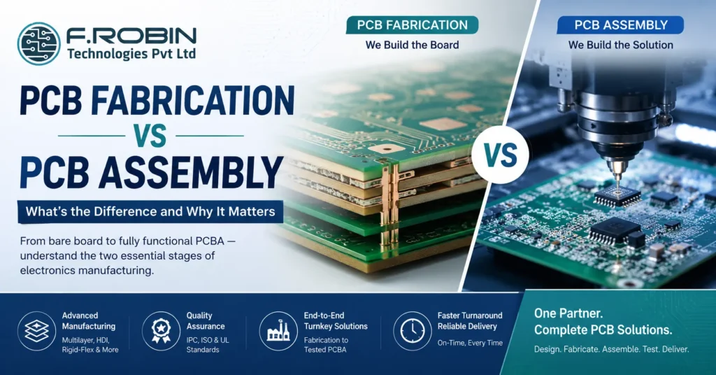
PCB fabrication vs PCB assembly these two terms appear constantly in electronics manufacturing, often interchangeably and almost always incorrectly. If you have ever sent a quote request to a manufacturer and been unsure whether to ask for “fabrication,” “assembly,” or both, this guide will clear that up completely.
In short: fabrication makes the board, while assembly populates it. Together, they produce a functional PCBA. However, the details of each process the different expertise they require, the distinct quality standards they are held to, and the cost implications of each are worth understanding in full, especially if you are about to place your first manufacturing order or are evaluating new suppliers.
1. What Is PCB Fabrication?
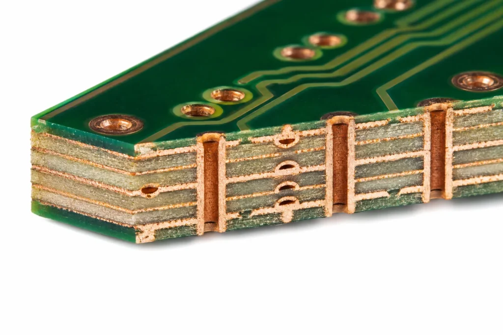
PCB fabrication is the process of manufacturing the bare printed circuit board — the physical substrate with copper traces, drilled holes, plated vias, solder mask, and silkscreen — but with no components attached.
Think of it as building the foundation of a building before any furniture goes in. The board comes out of fabrication as a flat, component-free physical object that carries the electrical connectivity your design requires. Every trace, pad, via, and plane is in place, yet nothing is soldered and nothing is placed.
What Happens During PCB Fabrication
Preparing the Inner Layers
Step 1 — Inner layer imaging (multilayer boards) Copper-clad laminate sheets are coated with photoresist. Next, UV light exposes the circuit pattern onto the resist through a film or laser direct imaging (LDI) system. Unexposed resist is then washed away, and the exposed copper is etched off — leaving only the copper traces of that layer.
Step 2 — Lamination For multilayer boards, the individual inner layers are stacked with prepreg (glass-fibre resin sheets) between them and pressed together under heat and pressure in a lamination press. As a result, all layers bond into a single rigid substrate.
Step 3 — Drilling CNC drilling machines drill holes through the laminated stack for through-hole component leads, via connections between layers, and mechanical mounting holes. In addition, high-density boards may use laser drilling for microvias where standard CNC cannot reach the required diameter.
Step 4 — Plating The drilled holes are electrolessly copper-plated to create electrical conductivity between layers. This plating step is precisely what makes a via a via — a copper-plated barrel connecting two or more copper layers through a drilled hole.
Finishing the Board Surface
Step 5 — Outer layer imaging and etching Following inner layer processing, the outer copper layers go through the same imaging and etching process, defining the surface traces and pads.
Step 6 — Solder mask application A liquid photoimageable solder mask (LPI) is applied over the entire board surface, then exposed and developed to open only the pad areas. Consequently, the traces remain protected by the green (or black, red, or blue) coating you see on a finished PCB, which prevents solder bridging during assembly and protects copper from oxidation.
Step 7 — Surface finish The exposed copper pads receive a surface finish to prevent oxidation and ensure good solderability. Common finishes include:
- HASL — cost-effective, suitable for most standard designs
- ENIG — flat and solderable, required for fine-pitch SMD and BGA pads
- OSP — thin organic coating, lowest cost, but with limited shelf life
- Hard gold — reserved for edge connectors and contact fingers
Step 8 — Silkscreen printing Reference designators, component outlines, polarity markers, logos, and other markings are printed on the board using white or yellow ink. This silkscreen layer is what your assembler and operators use as a visual reference during assembly and inspection.
Step 9 — Electrical testing Every fabricated board is electrically tested — either by flying probe or bed of nails — to verify that all nets are continuous and no unintended shorts exist. Importantly, a board that fails electrical test at fabrication never reaches assembly.
Step 10 — Visual inspection, routing, and delivery Finally, boards are inspected visually and under AOI, then routed from the production panel into individual boards or arrays and packaged for delivery.
2. What Is PCB Assembly?
PCB assembly (PCBA) is the process of soldering electronic components onto the fabricated bare board to create a functional electronic circuit. Whereas fabrication builds the substrate, assembly populates it.
The assembled board — called a PCBA (Printed Circuit Board Assembly) — is the finished functional unit: the thing that goes into your product, gets tested, and performs the electronic function your design was created for.
What Happens During PCB Assembly
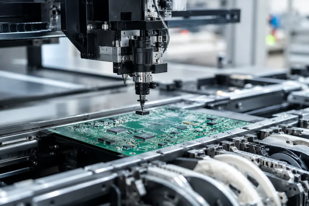
Step 1 — Solder paste stencil printing A laser-cut stainless steel stencil is aligned over the bare board. Solder paste is then squeegeed across the stencil, depositing precise volumes of paste only on the pad areas through the stencil apertures. Critically, paste volume and consistency at this step directly determines solder joint quality downstream.
Step 2 — SMT component placement (pick and place) An automated pick-and-place machine retrieves components from reels, trays, and tubes, then places them on the solder-pasted pads with micron-level accuracy. Modern machines handle components as small as 0201 (0.6mm × 0.3mm) and manage fine-pitch BGAs, QFNs, and multi-pin connectors in the same pass.
Step 3 — Reflow soldering The populated board travels through a multi-zone reflow oven on a conveyor. Throughout this stage, the temperature profile — preheat, thermal soak, reflow peak, and cooling — is precisely controlled to melt and resolidify the solder paste into reliable intermetallic solder joints without damaging components. Profiles are customised per board based on component thermal sensitivity and paste specification.
Step 4: Removed “through-hole components” → replaced with “components” (the step heading already tells the reader it’s through-hole) Step 5: Replaced “Through-hole component leads on the bottom of the board are subsequently soldered” → replaced with “Once insertion is complete, the leads on the bottom of the board are soldered” — breaks the consecutive pattern and adds a transition word Yoast will also count
Step 6 — Inspection AOI (Automated Optical Inspection) scans every board for missing components, wrong orientation, solder bridges, lifted leads, and insufficient solder. Additionally, X-ray inspection checks hidden solder joints on BGA and QFN packages, while visual inspection by trained operators provides a final check.
Step 7 — Testing Electrical testing (flying probe or ICT) verifies circuit continuity and component values. Furthermore, functional testing powers up the board and exercises it against a test specification to confirm it performs its intended function.
Step 8 — Cleaning and finishing Flux residue is cleaned — an essential step for high-frequency, medical, and aerospace boards. Conformal coating is applied if required for environmental protection. Finally, boards are labelled, serialised, and packaged for delivery.
3. PCB Fabrication vs PCB Assembly — Side by Side
Here is a clear comparison of both processes across every dimension that matters:
| Factor | PCB Fabrication | PCB Assembly |
|---|---|---|
| What it produces | Bare board — no components | Populated board (PCBA) — all components soldered |
| Input materials | Copper-clad laminate, prepreg, chemicals | Bare PCB, components, solder paste, stencil |
| Key processes | Lamination, drilling, plating, etching, solder mask | Paste printing, pick & place, reflow, wave solder, inspection |
| Key equipment | CNC drills, lamination presses, etching lines, AOI | Stencil printers, pick & place, reflow ovens, wave solder, AOI, X-ray |
| Quality standard | IPC-6012 (rigid boards), IPC-6013 (flex) | IPC-A-610 (workmanship), J-STD-001 (soldering) |
| Primary skill | Chemical engineering, precision machining | Electronics assembly, soldering, inspection |
| Output | Bare PCB or PCB panel | Assembled and tested PCBA |
| Can it function? | No — no components | Yes — ready for integration or end use |
| Lead time (India) | 15–25 working days | 5–20 working days (after bare board ready) |
4. Can the Same Company Do Both?
Yes — and when they do, it is called turnkey PCB manufacturing. A turnkey supplier takes your design files (Gerbers for fabrication + BOM and centroid for assembly) and delivers finished, tested PCBAs. As a result, you deal with one supplier, one point of contact, and one quality system for both processes.
The alternative is split sourcing: ordering bare boards from one fabricator and shipping them to a separate assembly house. Some teams follow this route when they have an established relationship with a specific fabricator or need a specialised material — such as Rogers, PTFE, or thick copper — that their preferred assembler cannot fabricate in-house.
Advantages of turnkey (single supplier for both):
- Simpler logistics — one order, one delivery
- No risk of board damage in transit between fab and assembly
- Assembler can flag fabrication quality issues before assembly begins
- Single accountability if defects arise — no blame-shifting between suppliers
- Often faster overall turnaround
Advantages of split sourcing:
- Access to specialised fabricators for unusual materials or very tight specs
- Flexibility to dual-source fabrication for supply chain resilience
- Potentially cheaper if your volume warrants dedicated fab relationships
For most hardware teams — particularly startups and mid-size OEMs — turnkey is the right starting point. The logistics savings and simplified accountability more than offset any marginal cost difference.
F.Robin Technologies provides fully integrated PCB fabrication and assembly services from a single facility in Madurai, Tamil Nadu — covering multilayer, HDI, rigid-flex, and metal-core boards, all assembled and tested to IPC, ISO, and UL standards. Learn more at frobintech.com/pcb-manufacturing.
5. Cost Breakdown: Fabrication vs Assembly
Understanding where the money goes in each process helps you optimise your BOM, design, and order strategy.
| Factor | Impact on Cost |
|---|---|
| Layer count | High — each additional layer adds lamination, imaging, and drilling cost |
| Board size | Moderate — larger boards yield fewer per panel |
| Minimum feature size | High — tighter traces and spaces require more precise (and expensive) equipment |
| Surface finish | Moderate — ENIG adds 20–40% over HASL |
| Material | High — Rogers, PTFE, high-Tg FR4 are significantly more expensive than standard FR4 |
| Quantity | Significant — setup cost amortised over more boards |
| Lead time | Moderate — quick-turn adds 30–60% premium |
| Factor | Impact on Cost |
|---|---|
| Component cost | Usually dominant — 50–70% of total PCBA cost |
| Component count | High — more placements = more machine time |
| Package complexity | High — BGAs cost more to place, inspect, and verify than passive 0402s |
| Double-sided assembly | Moderate — second reflow pass adds time and cost |
| Through-hole count | High — manual insertion adds ₹2–8 per component in labour |
| Testing method | Moderate to high — AOI is low cost; ICT fixtures are ₹50K–₹3L NRE |
| Volume | Significant — NRE amortised, component pricing improves at volume |
6. Common Mistakes When Ordering PCB Fabrication and Assembly
Mistake 1: Sending assembly files to a fabricator (or vice versa) Fabricators need Gerber files, drill files, and board stackup specifications, whereas assemblers need a BOM with MPNs and a centroid/XY placement file. Confusing the two routinely delays orders by several days.
Mistake 2: Not specifying the IPC class IPC-A-610 Class 2 and Class 3 have different acceptance criteria for the same defect. Without a specified class, your assembler will default to Class 2 — which may not be acceptable for medical, automotive, or safety-critical applications.
Mistake 3: Ordering fabrication without a DFM review A board design can be electrically correct yet still impossible or expensive to fabricate — due to minimum annular ring violations, via aspect ratios that exceed the fab’s capability, or solder mask slivers that break during processing. Running a DFM review before fabrication catches these issues before they become costly scrap.
Mistake 4: Not providing ENIG for BGA and fine-pitch components HASL finish leaves an uneven surface that causes BGA placement issues and fine-pitch bridging. Therefore, any board with components at 0.5mm pitch or below — or any BGA — requires ENIG or OSP surface finish, not HASL.
Mistake 5: Treating fabrication and assembly lead times as independent If fabrication takes 7 days and assembly takes 10 days, your total lead time is at minimum 17 days — plus transit time between suppliers if split sourcing. Turnkey suppliers compress this significantly because they can start assembly preparation (stencil, programming, component procurement) while fabrication is still running.
For design support before fabrication, F.Robin Technologies also provides PCB layout and design services — visit frobintech.com/pcb-layout-design to learn more.
Conclusion
PCB fabrication and PCB assembly are two distinct manufacturing processes, each with its own equipment, expertise, quality standards, and cost structure. Fabrication builds the board. Assembly populates it. Together — in a well-managed turnkey process — they deliver a tested, functional PCBA ready for integration into your product.
Understanding the difference is not just academic. It directly affects how you specify your orders, evaluate supplier quotes, plan your timeline, and manage quality across both processes.
F.Robin Technologies delivers both fabrication and assembly under one roof — multilayer, HDI, rigid-flex, and metal-core PCBs manufactured and assembled to IPC, ISO, and UL standards, from our facility in Madurai, Tamil Nadu.
Have a Question About PCB Fabrication or Assembly?
Our engineering team is ready to review your design, answer your questions, and guide you from bare board to finished PCBA.
Contact Our Team