
PCB Fabrication vs PCB Assembly: What’s the Difference and Why It Matters
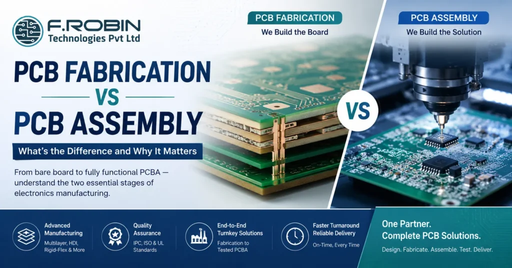
Introduction PCB fabrication vs PCB assembly these two terms appear constantly in electronics manufacturing, often interchangeably and almost always incorrectly. If you have ever sent a quote request to a manufacturer and been unsure whether to ask for “fabrication,” “assembly,” or both, this guide will clear that up completely. In short: fabrication makes the board, while assembly populates it. Together, they produce a functional PCBA. However, the details of each process the different expertise they require, the distinct quality standards they are held to, and the cost implications of each are worth understanding in full, especially if you are about to place your first manufacturing order or are evaluating new suppliers. 1. What Is PCB Fabrication? PCB fabrication is the process of manufacturing the bare printed circuit board — the physical substrate with copper traces, drilled holes, plated vias, solder mask, and silkscreen — but with no components attached. Think of it as building the foundation of a building before any furniture goes in. The board comes out of fabrication as a flat, component-free physical object that carries the electrical connectivity your design requires. Every trace, pad, via, and plane is in place, yet nothing is soldered and nothing is placed. What Happens During PCB Fabrication Preparing the Inner Layers Step 1 — Inner layer imaging (multilayer boards) Copper-clad laminate sheets are coated with photoresist. Next, UV light exposes the circuit pattern onto the resist through a film or laser direct imaging (LDI) system. Unexposed resist is then washed away, and the exposed copper is etched off — leaving only the copper traces of that layer. Step 2 — Lamination For multilayer boards, the individual inner layers are stacked with prepreg (glass-fibre resin sheets) between them and pressed together under heat and pressure in a lamination press. As a result, all layers bond into a single rigid substrate. Step 3 — Drilling CNC drilling machines drill holes through the laminated stack for through-hole component leads, via connections between layers, and mechanical mounting holes. In addition, high-density boards may use laser drilling for microvias where standard CNC cannot reach the required diameter. Step 4 — Plating The drilled holes are electrolessly copper-plated to create electrical conductivity between layers. This plating step is precisely what makes a via a via — a copper-plated barrel connecting two or more copper layers through a drilled hole. Finishing the Board Surface Step 5 — Outer layer imaging and etching Following inner layer processing, the outer copper layers go through the same imaging and etching process, defining the surface traces and pads. Step 6 — Solder mask application A liquid photoimageable solder mask (LPI) is applied over the entire board surface, then exposed and developed to open only the pad areas. Consequently, the traces remain protected by the green (or black, red, or blue) coating you see on a finished PCB, which prevents solder bridging during assembly and protects copper from oxidation. Step 7 — Surface finish The exposed copper pads receive a surface finish to prevent oxidation and ensure good solderability. Common finishes include: Step 8 — Silkscreen printing Reference designators, component outlines, polarity markers, logos, and other markings are printed on the board using white or yellow ink. This silkscreen layer is what your assembler and operators use as a visual reference during assembly and inspection. Step 9 — Electrical testing Every fabricated board is electrically tested — either by flying probe or bed of nails — to verify that all nets are continuous and no unintended shorts exist. Importantly, a board that fails electrical test at fabrication never reaches assembly. Step 10 — Visual inspection, routing, and delivery Finally, boards are inspected visually and under AOI, then routed from the production panel into individual boards or arrays and packaged for delivery. 2. What Is PCB Assembly? PCB assembly (PCBA) is the process of soldering electronic components onto the fabricated bare board to create a functional electronic circuit. Whereas fabrication builds the substrate, assembly populates it. The assembled board — called a PCBA (Printed Circuit Board Assembly) — is the finished functional unit: the thing that goes into your product, gets tested, and performs the electronic function your design was created for. What Happens During PCB Assembly Step 1 — Solder paste stencil printing A laser-cut stainless steel stencil is aligned over the bare board. Solder paste is then squeegeed across the stencil, depositing precise volumes of paste only on the pad areas through the stencil apertures. Critically, paste volume and consistency at this step directly determines solder joint quality downstream. Step 2 — SMT component placement (pick and place) An automated pick-and-place machine retrieves components from reels, trays, and tubes, then places them on the solder-pasted pads with micron-level accuracy. Modern machines handle components as small as 0201 (0.6mm × 0.3mm) and manage fine-pitch BGAs, QFNs, and multi-pin connectors in the same pass. Step 3 — Reflow soldering The populated board travels through a multi-zone reflow oven on a conveyor. Throughout this stage, the temperature profile — preheat, thermal soak, reflow peak, and cooling — is precisely controlled to melt and resolidify the solder paste into reliable intermetallic solder joints without damaging components. Profiles are customised per board based on component thermal sensitivity and paste specification. Step 4: Removed “through-hole components” → replaced with “components” (the step heading already tells the reader it’s through-hole) Step 5: Replaced “Through-hole component leads on the bottom of the board are subsequently soldered” → replaced with “Once insertion is complete, the leads on the bottom of the board are soldered” — breaks the consecutive pattern and adds a transition word Yoast will also count Step 6 — Inspection AOI (Automated Optical Inspection) scans every board for missing components, wrong orientation, solder bridges, lifted leads, and insufficient solder. Additionally, X-ray inspection checks hidden solder joints on BGA and QFN packages, while visual inspection by trained operators provides a final check. Step 7 — Testing Electrical testing (flying probe or ICT) verifies circuit continuity and component values. Furthermore,
SMT vs Through-Hole Assembly: Which Soldering Method Is Right for Your PCB?
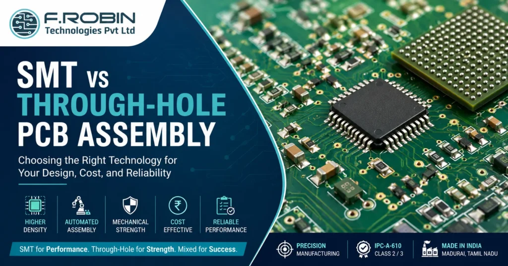
Introduction When it comes to SMT vs through-hole assembly, choosing the wrong method for your PCB can quietly inflate your manufacturing cost, delay your timeline, and create reliability problems that only surface after your product ships. Every PCB design reaches a moment where the engineer has to decide: surface mount, through-hole, or both? It sounds like a technical detail, but it directly affects your assembly cost, board size, mechanical reliability, and how quickly you can get boards back from your manufacturer. This guide breaks down both methods clearly — what they are, where each one wins, and how to make the right choice for your specific application. Whether you are designing a compact IoT sensor, a ruggedised industrial controller, or a power electronics board, understanding SMT vs through-hole assembly is a decision that matters more than most teams realise. 1. What Is SMT (Surface Mount Technology)? Surface mount technology places components directly onto the surface of the PCB. Components have no leads that pass through the board — instead they have flat pads or small solder balls that sit on copper pads on the top or bottom surface, held in place by solder paste and reflowed in an oven. Common SMT component packages The smallest SMT passives in common use today — 01005 (0.4mm × 0.2mm) — are about the size of a grain of sand. BGA packages hide hundreds of solder balls underneath the IC body in a grid matrix, requiring X-ray inspection to verify assembly quality. SMT is the dominant assembly technology for virtually all modern consumer electronics, IoT devices, smartphones, and computing hardware. 2. What Is Through-Hole Assembly? Through-hole assembly uses components with wire leads that pass through drilled holes in the PCB. The leads are soldered on the opposite side of the board — either by wave soldering, selective soldering, or hand soldering. Through-hole was the dominant PCB assembly method from the 1950s through the late 1980s. Today it is used selectively, primarily for components where mechanical strength, high current capacity, or replaceability matter more than board density. Common through-hole component packages Through-hole components are still the right choice for connectors that will be plugged and unplugged repeatedly, high-voltage or high-current components, and components that must survive mechanical vibration or shock. 3. Key Differences — Board Density, Mechanical Strength, Cost, Speed Here is how the two technologies compare across the metrics that matter most in production decisions: Factor SMT Through-hole Board Density Very high — components on both sides, no drill holes required Low — holes reduce routing space; components typically one side only Component Size Extremely small (down to 0.4mm × 0.2mm) Larger — requires lead pitch and hole clearance Mechanical Strength Moderate — relies on solder joint to PCB surface High — lead passes through board and is soldered on both sides Assembly Speed Very fast — automated pick and place at 20,000–60,000 cph Slower — insertion requires machines or manual operators Assembly Cost (Volume) Low at high volume — fully automated Higher — manual or semi-automated insertion adds labour Prototype Cost Moderate — stencil and setup NRE Lower for hand-soldered prototypes Rework / Repair Harder — requires hot air, tweezers, fine-pitch tools Easier — leads can be clipped, reflowed, replaced with standard tools Vibration Resistance Lower Higher — lead-through-hole provides mechanical anchor 4. When to Use SMT Choose SMT as your primary assembly method when: You need small form factor. SMT components are 10–100× smaller than their through-hole equivalents. A 0402 resistor is 1.0mm × 0.5mm. The SMD equivalent of a 16-pin DIP IC might be a QFN at 3mm × 3mm. If your board needs to fit inside a compact enclosure, SMT is not optional — it is the only viable path. You are designing for high-volume production. Automated SMT lines can place and solder thousands of components per hour with minimal human intervention. Unit cost drops sharply at volume because the machine cost is amortised across a large number of builds. Pick-and-place machines handle component placement; reflow ovens handle soldering — no manual intervention required. You are building IoT or consumer electronics. Virtually all IoT modules, Bluetooth chips, Wi-Fi SoCs, microcontrollers, and sensors are only available in SMT packages. If your BOM includes an ESP32, nRF52, STM32, or similar, you are already committed to SMT. You want double-sided assembly. SMT components can be placed and reflowed on both sides of the board, dramatically increasing routing and component density without increasing board size. You need controlled impedance or high-frequency routing. Drill holes in through-hole designs create via stubs and discontinuities in signal paths. All-SMT designs with controlled via placement offer much better signal integrity for RF, high-speed digital, and power switching applications. 5. When to Use Through-Hole Through-hole is the right choice — even in predominantly SMT designs — for specific component types: High-stress connectors. USB ports, D-sub connectors, RJ45 jacks, and power barrel jacks that are plugged and unplugged repeatedly put mechanical stress on the solder joint. Through-hole soldering anchors the connector mechanically through the board rather than relying only on surface adhesion. For consumer products with daily use, through-hole connectors last significantly longer. Power components. Large electrolytic capacitors (≥100µF, 25V+), wirewound resistors, high-current inductors, and power transistors in TO-220 or TO-247 packages all exist in through-hole form for good reason — they handle heat and current that would stress smaller SMD packages. Heat sinking through the lead and board is also more effective. High-vibration environments. Automotive electronics, industrial machinery, robotics, and aerospace applications expose boards to continuous mechanical vibration. Through-hole components, with their leads soldered on both board sides, resist mechanical loosening far better than SMT joints under sustained vibration. Prototyping with socketed ICs. Through-hole DIP ICs can be socketed — inserted into ZIF (Zero Insertion Force) or DIP sockets — allowing you to swap microcontrollers, EEPROMs, or op-amps during development without soldering and desoldering repeatedly. For R&D boards where component swaps are expected, this is invaluable. High-voltage isolation. Safety-critical applications requiring specific creepage and clearance distances between high-voltage
Turnkey PCB Assembly Services in India: Everything You Need to Know Before Placing an Order
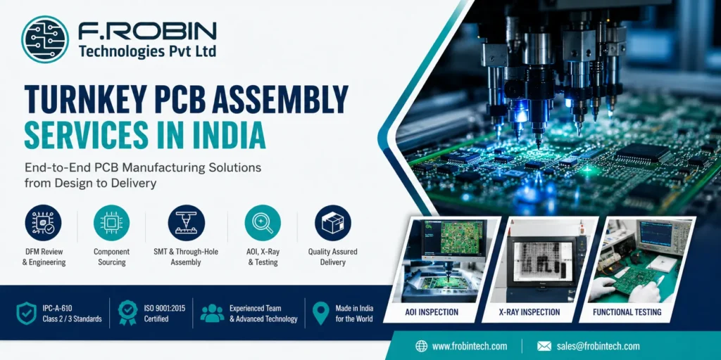
Introduction Turnkey PCB assembly services India are becoming essential for hardware startups, OEMs, R&D teams, and electronics companies looking for reliable PCB manufacturing, component sourcing, SMT assembly, testing, and fast production support under one roof. Whether you are building a prototype, pilot batch, or full production run, choosing the right turnkey PCB assembly partner directly affects product quality, lead times, and manufacturing cost. So you have a PCB design ready. The Gerbers are exported, the BOM is drafted, and you need someone to build it. You search for PCB assembly services in India and are immediately confronted with unfamiliar terms like turnkey, partial turnkey, consignment, PCBA, SMT, AOI, and functional testing. This guide explains everything you need to know before placing an order for turnkey PCB assembly services in India, including the assembly process, testing methods, file preparation, pricing factors, and how to choose the right EMS manufacturing partner. 1. What Are Turnkey PCB Assembly Services in India? Turnkey PCB assembly means you hand off the job completely — design files, BOM, and sometimes the bare PCBs — and receive assembled, tested boards in return. The manufacturer handles component sourcing, procurement, kitting, solder paste printing, pick-and-place, reflow, inspection, and often functional testing. The Three Models Full Turnkey You supply only design files (Gerbers, BOM, centroid file). The manufacturer procures all components, fabricates bare boards, assembles, inspects, and ships finished boards. The most hands-off and most popular option for startups and hardware teams without procurement infrastructure. Partial Turnkey (Kitted Assembly) You supply some components — long-lead items or proprietary parts — and the manufacturer supplies the rest. Common for products with custom ICs, specialised sensors, or parts under NDA. Consignment (CM-Only) You supply everything: bare boards, all components, stencil, sometimes solder paste. The manufacturer provides only assembly labour and equipment. Used by large OEMs with established supply chains. 2. The Turnkey PCBA Process End to End 3. SMT vs Through-Hole Assembly in the Turnkey Context Most modern PCBs are predominantly SMT, but boards with both SMT and through-hole components require understanding the two-pass process. Pure SMT boards are the fastest and most cost-effective to assemble. The entire process is automated. If your design can be fully SMT — using SMD connectors, SMD electrolytic capacitors, SMD crystals — do it. Mixed technology boards (SMT + through-hole) require two passes: SMT components are placed and reflowed first; through-hole components are then inserted and selectively soldered. This adds time and cost, but is often unavoidable for high-current power components and ruggedised connectors. Pure through-hole boards are rare today and are assembled by hand insertion and wave soldering. 4. AOI, X-Ray, and Functional Testing in Turnkey Lines Testing is where many low-cost assemblers cut corners — and where you pay the price when field failures occur. Automated Optical Inspection (AOI) AOI machines use high-resolution cameras and image processing to inspect every solder joint and component placement. AOI catches: What AOI misses: Hidden solder joints (BGA balls, QFN thermal pads), electrical opens/shorts that don’t show optically, and functional failures. X-Ray Inspection X-ray is essential for BGA, QFN, and LGA packages where solder joints are hidden under the component body. It reveals: For any board with a BGA or QFN component, X-ray inspection is mandatory, not optional. In-Circuit Testing (ICT) ICT uses a “bed of nails” fixture with spring-loaded probes contacting test points to measure component values and check for shorts/opens. Fast and thorough but requires a custom fixture costing ₹50,000–₹3,00,000+. Economical only at 500+ units. Flying Probe Testing Flying probe uses movable probes without a custom fixture — ideal for prototype and low-volume runs. Slower than ICT but fixture-free and catches shorts, opens, and component value errors. Functional Testing (FCT) FCT powers up the assembled board and exercises it exactly as in the final product. A custom test jig interfaces with the board’s connectors and I/O, stimulates inputs, and measures outputs. FCT is the only test method that definitively proves the board works. Recommended Testing Strategy by Volume Production Volume Recommended Tests 1–10 Units (Prototype) Visual Inspection + Flying Probe Testing + Functional Circuit Testing (FCT) 10–100 Units (Pilot Run) AOI + X-ray Inspection (for BGA/QFN) + Functional Circuit Testing (FCT) 100–1,000 Units AOI + X-ray Inspection + ICT or Flying Probe Testing + Functional Circuit Testing (FCT) 1,000+ Units (Mass Production) AOI + X-ray Inspection + ICT + Functional Circuit Testing (FCT) + Burn-In Testing 5. Component Sourcing in India — Counterfeit Risk, and Approved Vendor Lists Component sourcing is one of the most overlooked aspects of turnkey assembly — and one of the most consequential. Counterfeit Component Risk Counterfeit electronic components are a real problem, especially sourced through grey-market channels. Counterfeits can fail immediately, pass initial testing and fail in the field, or cause safety issues. To mitigate risk: Approved Vendor Lists (AVL) An AVL is a list of approved manufacturers and distributors for each BOM line item. For prototype runs, authorised distributors are sufficient. For production, define and submit your AVL with your production BOM. 6. How to Prepare Files for Turnkey Assembly Poor file preparation is the single most common cause of delays, miscommunications, and assembly errors. Gerber Files (RS-274X Format) Include: all copper layers, solder mask layers (top and bottom), silkscreen layers, drill file (Excellon format), and board outline. Name layers clearly. Double-check: Bill of Materials (BOM) Every component must include: A BOM with only generic descriptions (“100nF capacitor, 0402”) forces sourcing assumptions that may not match your design intent. Always provide MPNs. Centroid / Pick-and-Place / XY File Contains reference designator, X and Y coordinates, rotation angle, and board side for every SMT component. Export from your PCB tool and verify the coordinate origin matches your Gerber origin. A mismatch causes your assembler to manually adjust every component location. Assembly Drawing A 2D PDF showing top and bottom of the assembled board with reference designators visible, polarity markings for diodes and electrolytic capacitors, and any special assembly notes. Test Specification (for FCT) Describe what the board must do, how
