
Introduction
Turnkey PCB assembly services India are becoming essential for hardware startups, OEMs, R&D teams, and electronics companies looking for reliable PCB manufacturing, component sourcing, SMT assembly, testing, and fast production support under one roof. Whether you are building a prototype, pilot batch, or full production run, choosing the right turnkey PCB assembly partner directly affects product quality, lead times, and manufacturing cost.
So you have a PCB design ready. The Gerbers are exported, the BOM is drafted, and you need someone to build it. You search for PCB assembly services in India and are immediately confronted with unfamiliar terms like turnkey, partial turnkey, consignment, PCBA, SMT, AOI, and functional testing.
This guide explains everything you need to know before placing an order for turnkey PCB assembly services in India, including the assembly process, testing methods, file preparation, pricing factors, and how to choose the right EMS manufacturing partner.
1. What Are Turnkey PCB Assembly Services in India?
Turnkey PCB assembly means you hand off the job completely — design files, BOM, and sometimes the bare PCBs — and receive assembled, tested boards in return. The manufacturer handles component sourcing, procurement, kitting, solder paste printing, pick-and-place, reflow, inspection, and often functional testing.
The Three Models
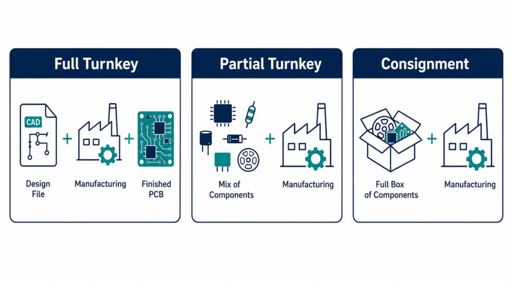
Full Turnkey You supply only design files (Gerbers, BOM, centroid file). The manufacturer procures all components, fabricates bare boards, assembles, inspects, and ships finished boards. The most hands-off and most popular option for startups and hardware teams without procurement infrastructure.
Partial Turnkey (Kitted Assembly) You supply some components — long-lead items or proprietary parts — and the manufacturer supplies the rest. Common for products with custom ICs, specialised sensors, or parts under NDA.
Consignment (CM-Only) You supply everything: bare boards, all components, stencil, sometimes solder paste. The manufacturer provides only assembly labour and equipment. Used by large OEMs with established supply chains.
2. The Turnkey PCBA Process End to End
Understanding what happens between uploading your files and receiving boards helps you catch problems early and communicate better with your assembly partner.
- Design File Review and DFM Check
Before a component is ordered, a competent assembler runs a DFM (Design for Manufacturability) check on your Gerbers and BOM. This flags issues like pads too small for the reflow process, insufficient clearance between components, missing courtyard layers, or components that are end-of-life.
What to expect: A DFM report listing issues by severity, within 24–48 hours of submission. Do not skip this step. A design that cannot be manufactured reliably costs far more to fix after production than before it. - BOM Processing and Component Sourcing
Your BOM is cross-referenced against distributor inventory to verify component availability and lead times, identify any end-of-life or long-lead parts, recommend approved substitutes for out-of-stock components, and ensure that all component footprints correctly match the PCB pad layout before assembly begins.
- Bare PCB Fabrication or Procurement
For standard FR4 designs (4–6 layers, 100µm traces), fabrication typically takes 3–7 working days within India. High-complexity boards (8+ layers, HDI, controlled impedance, Rogers material) may take 10–15 working days. - Solder Paste Stencil Preparation
A laser-cut stainless steel stencil is made from your solder paste layer (.gtp Gerber file). Stencil thickness typically 100–150µm for standard SMD, down to 80µm for fine-pitch QFN and BGAs determines paste volume. - Solder Paste Printing
The bare PCB is aligned to the stencil in an automatic stencil printer. Paste is squeegeed across the stencil, depositing precise solder paste volumes on each pad. Paste volume consistency directly determines soldering quality.
- Pick and Place
An automated pick-and-place machine retrieves components from tape reels, trays, or tubes and places them on pasted pads with micron-level accuracy. Modern machines handle components from 0201 passives (0.6mm × 0.3mm) to 50mm+ connectors at 20,000–60,000 placements per hour.
- Reflow Soldering
The populated board travels through a reflow oven. The oven profile — preheat, soak, reflow, and cooling zones — melts and resolidifies the solder paste, forming reliable joints. The profile is customised per board based on component thermal mass and solder paste specification.
- Through-Hole Insertion and Wave/Selective Soldering
Through-hole components (connectors, electrolytic capacitors, transformers) are inserted after reflow and soldered by wave soldering or selective soldering.
- Inspection and Testing
Covered in detail in Section 4. At minimum, expect visual inspection and AOI. For production builds, functional testing is mandatory.
- Cleaning, Conformal Coating, and Packaging
Boards are cleaned to remove flux residue, optionally coated with conformal coating for environmental protection, and packaged for shipment.
3. SMT vs Through-Hole Assembly in the Turnkey Context
Most modern PCBs are predominantly SMT, but boards with both SMT and through-hole components require understanding the two-pass process.
Pure SMT boards are the fastest and most cost-effective to assemble. The entire process is automated. If your design can be fully SMT — using SMD connectors, SMD electrolytic capacitors, SMD crystals — do it.
Mixed technology boards (SMT + through-hole) require two passes: SMT components are placed and reflowed first; through-hole components are then inserted and selectively soldered. This adds time and cost, but is often unavoidable for high-current power components and ruggedised connectors.
Pure through-hole boards are rare today and are assembled by hand insertion and wave soldering.
4. AOI, X-Ray, and Functional Testing in Turnkey Lines
Testing is where many low-cost assemblers cut corners — and where you pay the price when field failures occur.
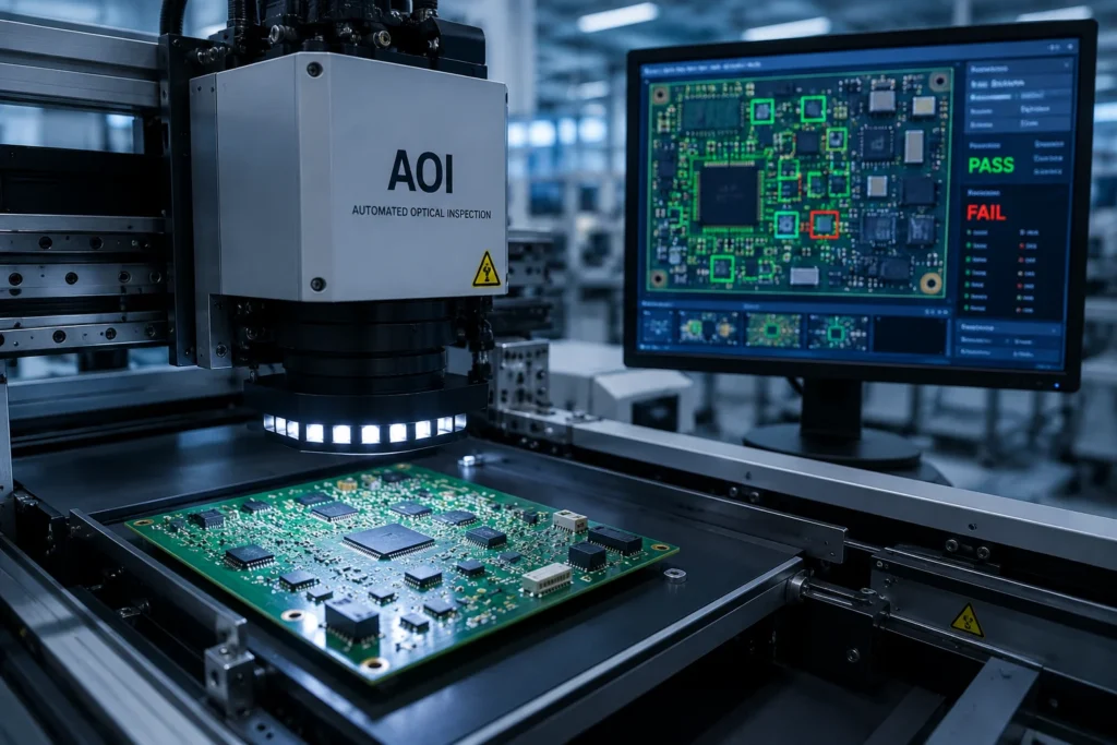
Automated Optical Inspection (AOI)
AOI machines use high-resolution cameras and image processing to inspect every solder joint and component placement. AOI catches:
- Missing components
- Wrong component orientation or polarity
- Lifted leads
- Solder bridges
- Insufficient solder (cold joints)
- Tombstoned components
What AOI misses: Hidden solder joints (BGA balls, QFN thermal pads), electrical opens/shorts that don’t show optically, and functional failures.
X-Ray Inspection
X-ray is essential for BGA, QFN, and LGA packages where solder joints are hidden under the component body. It reveals:
- BGA ball collapse and shape
- Voiding in BGA and QFN joints
- Hidden solder bridges
- Missing balls
For any board with a BGA or QFN component, X-ray inspection is mandatory, not optional.
In-Circuit Testing (ICT)
ICT uses a “bed of nails” fixture with spring-loaded probes contacting test points to measure component values and check for shorts/opens. Fast and thorough but requires a custom fixture costing ₹50,000–₹3,00,000+. Economical only at 500+ units.
Flying Probe Testing
Flying probe uses movable probes without a custom fixture — ideal for prototype and low-volume runs. Slower than ICT but fixture-free and catches shorts, opens, and component value errors.
Functional Testing (FCT)
FCT powers up the assembled board and exercises it exactly as in the final product. A custom test jig interfaces with the board’s connectors and I/O, stimulates inputs, and measures outputs. FCT is the only test method that definitively proves the board works.
Recommended Testing Strategy by Volume
| Production Volume | Recommended Tests |
|---|---|
| 1–10 Units (Prototype) | Visual Inspection + Flying Probe Testing + Functional Circuit Testing (FCT) |
| 10–100 Units (Pilot Run) | AOI + X-ray Inspection (for BGA/QFN) + Functional Circuit Testing (FCT) |
| 100–1,000 Units | AOI + X-ray Inspection + ICT or Flying Probe Testing + Functional Circuit Testing (FCT) |
| 1,000+ Units (Mass Production) | AOI + X-ray Inspection + ICT + Functional Circuit Testing (FCT) + Burn-In Testing |
5. Component Sourcing in India — Counterfeit Risk, and Approved Vendor Lists
Component sourcing is one of the most overlooked aspects of turnkey assembly — and one of the most consequential.
Counterfeit Component Risk
Counterfeit electronic components are a real problem, especially sourced through grey-market channels. Counterfeits can fail immediately, pass initial testing and fail in the field, or cause safety issues. To mitigate risk:
- Authorised distributor sourcing only — Mouser, DigiKey, Arrow, Avnet
- Certificates of Conformance (CoC) for all critical components
- Date code and lot traceability records from your assembler
- Incoming inspection for sensitive or high-value ICs
Approved Vendor Lists (AVL)
An AVL is a list of approved manufacturers and distributors for each BOM line item. For prototype runs, authorised distributors are sufficient. For production, define and submit your AVL with your production BOM.
6. How to Prepare Files for Turnkey Assembly
Poor file preparation is the single most common cause of delays, miscommunications, and assembly errors.
Gerber Files (RS-274X Format)
Include: all copper layers, solder mask layers (top and bottom), silkscreen layers, drill file (Excellon format), and board outline. Name layers clearly. Double-check:
- Minimum trace width and spacing meet your fabricator’s capabilities
- All SMD pads have solder mask openings
- Board outline is a single, closed shape
- Drill file uses the same units (mm or inches) as your Gerbers
Bill of Materials (BOM)
Every component must include:
- Reference designator (R1, C4, U7) — matches silkscreen on board
- Manufacturer Part Number (MPN) — exact part, not a generic description
- Manufacturer name
- Description (value, package, rating)
- Quantity
- DNP flag for “Do Not Place” variants
A BOM with only generic descriptions (“100nF capacitor, 0402”) forces sourcing assumptions that may not match your design intent. Always provide MPNs.
Centroid / Pick-and-Place / XY File
Contains reference designator, X and Y coordinates, rotation angle, and board side for every SMT component. Export from your PCB tool and verify the coordinate origin matches your Gerber origin. A mismatch causes your assembler to manually adjust every component location.
Assembly Drawing
A 2D PDF showing top and bottom of the assembled board with reference designators visible, polarity markings for diodes and electrolytic capacitors, and any special assembly notes.
Test Specification (for FCT)
Describe what the board must do, how pass/fail is determined, power-on sequence, test stimulus, expected measurements, and acceptance criteria.
7. Questions to Ask Your Turnkey Assembly Partner
Before committing to an assembler, ask these questions directly.
Capability
- What is your minimum feature size for SMT (minimum pad pitch, minimum component size)?
- Do you have in-house X-ray for BGA inspection, or is it subcontracted?
- What EMS certifications do you hold — ISO 9001, IPC-A-610, IATF 16949, ISO 13485?
- What first-pass yield (FPY) do you achieve on SMT assembly?
Sourcing
- Do you source components exclusively from authorised distributors?
- Can you provide CoC and traceability records for all ICs?
- What is your process for handling component shortages or substitutions?
Quality
- What inspection steps are included as standard in your turnkey service?
- Can I visit your facility and see the production line?
- What is your rework or warranty policy if boards fail incoming inspection at my end?
Process
- Who is my point of contact and how quickly do you respond to queries?
- What are your lead times from file approval to shipment?
- How do you handle engineering changes (ECOs) during production?
- Do you provide board-level traceability — date code, lot number — on delivered units?
IP Protection
- Do you sign NDAs before reviewing design files?
- What is your policy on retaining Gerbers and BOMs after the project?
Conclusion
Turnkey PCB assembly in India works — when you choose the right partner and hand over complete, well-prepared files. Incomplete BOMs, skipped DFM checks, and vague test requirements are the three things that turn a smooth assembly run into an expensive rework cycle.
F.Robin Technologies handles the entire process — DFM review, authorised-distributor sourcing, SMT and through-hole assembly, AOI, X-ray inspection, and functional testing — all held to IPC-A-610 Class 2/3 workmanship standards, from our facility in Madurai, Tamil Nadu.
Need Help with PCB Assembly?
Get expert support for turnkey PCB assembly, SMT manufacturing, AOI inspection, and complete electronics manufacturing solutions for your next project.
Contact Our TeamFrequently Asked Questions
PCB (Printed Circuit Board) is the bare board — substrate with copper traces and pads, but no components. PCBA (PCB Assembly) is the completed board with all components soldered onto it.
Order at least 5, ideally 10. Manufacturing defects, bring-up failures, and test damage are all real possibilities. Having spares means a single bad board does not stop your entire development.
Yes — this is the partial turnkey or kitted model. Ship your components to the assembler with clear labelling (reference designator, MPN, quantity). Ensure components are in reflow-compatible packaging and not expired.
ENIG (Electroless Nickel Immersion Gold) is the best choice for fine-pitch SMD, BGAs, and boards sitting in inventory before assembly. HASL is cheaper and suitable for coarser designs. Lead-Free HASL is the RoHS-compliant version.
Turnkey PCB assembly services in India offer cost-effective electronics manufacturing, flexible prototype support, component sourcing assistance, SMT and through-hole assembly, and access to skilled engineering and testing teams for OEMs and hardware startups.
