
PCB Manufacturing: A Complete Guide From Gerbers to Boards
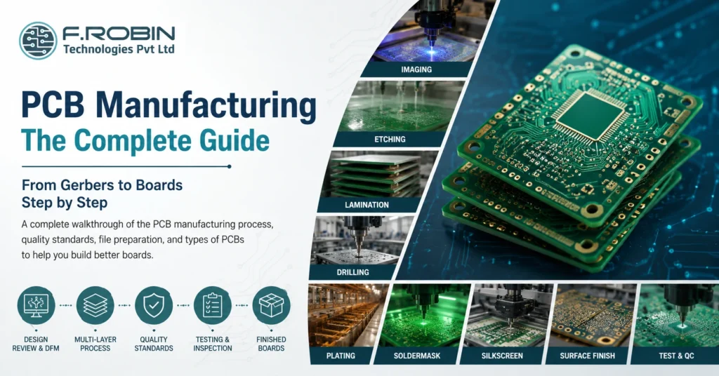
PCB manufacturing is the process of turning your design files into physical, ready-to-assemble circuit boards. It begins with Gerber data and ends with finished, tested boards — passing through imaging, etching, lamination, drilling, plating, and more along the way. If you have ever wondered what happens between hitting “export” and holding your board, this guide walks you through every stage. Understanding the process helps you design better boards, control cost, and choose the right partner. Whether you are comparing printed circuit board manufacturers or simply curious how circuit board manufacturing works, this complete guide takes you from Gerbers to boards, step by step. What Is PCB Manufacturing? PCB manufacturing, also called PCB fabrication, is the process of building a bare printed circuit board from design data. It transforms copper-clad laminate into a board with precise traces, layers, holes, and finishes, ready to receive components. The process is highly automated and tightly controlled, because tiny errors at this scale cause real failures. Most printed circuit board manufacturers follow IPC standards to guarantee consistent quality across every batch. As a result, a well-made board behaves exactly as the designer intended. It helps to remember what this stage does and does not include. Fabrication produces the empty board; it does not add components. That second step is assembly, which we cover in our guide to PCB assembly. Together, fabrication and assembly deliver a finished, working product. PCB Manufacturing vs PCB Assembly People often confuse these two stages, so let us be clear. Circuit board manufacturing creates the bare board — copper, layers, holes, soldermask, and finish. Assembly then solders components onto that board. In short: manufacturing makes the board; assembly populates it. Some vendors offer both as a turnkey service, while others specialize in one. Knowing the difference helps you scope quotes accurately and avoid surprises in your timeline. The PCB Manufacturing Process Step by Step Here is how pcb manufacturing turns Gerber files into finished boards. While details vary by factory, the core flow is consistent. Step 1: Design Review and DFM First, the factory reviews your Gerber or ODB++ files and runs a design-for-manufacturability (DFM) check. This catches issues like undersized traces or tight clearances before any material is cut. Step 2: Inner Layer Imaging and Etching Next, the inner copper layers are imaged with the circuit pattern. Etching then removes unwanted copper, leaving only the traces you designed. Precision here defines your final trace widths and impedance. Step 3: Lamination The etched inner layers are stacked with prepreg and copper foil, then bonded under heat and pressure. This lamination step fuses the layers into a single solid board — the heart of multilayer construction. Step 4: Drilling Now machines drill the holes for vias and through-hole parts. Modern drilling uses CNC and, for the smallest holes, lasers. Accurate drilling is essential for reliable connections between layers. Step 5: Plating and Through-Hole Metallization Copper plating coats the drilled holes, electrically connecting layers. This through-hole metallization is what turns a stack of separate layers into one connected circuit. Step 6: Outer Layer Imaging and Etching The outer layers are then imaged and etched, just like the inner layers, to form the surface traces and pads. Step 7: Soldermask and Silkscreen A soldermask is applied to protect the copper and prevent solder bridges, giving the board its familiar color. A silkscreen legend adds reference designators, logos, and markings. Step 8: Surface Finish A surface finish — such as ENIG, HASL protects exposed pads and ensures solderability during assembly. Step 9: Electrical Test and Final QC Finally, the boards are electrically tested for opens and shorts, inspected against IPC standards, then routed to their final shape and shipped. Clean files at the start make this final stage fast and trouble-free. Types of PCBs You Can Manufacture Pcb manufacturing supports many board types. The table below summarizes the main options. Type Description Typical Use Rigid 30 Layer Most products Multilayer Three or more layers Dense, high-speed designs Flexible 6 Layers Wearables, tight spaces Rigid-Flex 24 Layer Compact, reliable assemblies HDI High-density interconnect Fine-pitch, miniaturized boards Metal-Core Aluminum or copper base High-power, LED, and thermal-heavy applications Choosing the right type early shapes your cost and capability. For multilayer choices specifically, see our guide on multilayer PCB design. PCB Manufacturing Quality Standards Quality is not optional in circuit board manufacturing. Reputable printed circuit board manufacturers work to recognized standards: Asking which IPC class and certifications a supplier holds is a fast way to judge their quality discipline. A capable partner will state these clearly and back them with inspection reports. How to Prepare Your Files for PCB Manufacturing Clean data makes pcb manufacturing smooth and fast. Before you order, prepare a complete package: These outputs flow directly from your layout. For the upstream steps, see our printed circuit board design workflow guide, and finalize your data with professional PCB layout design services. How to Reduce PCB Manufacturing Cost You can lower cost without hurting quality by designing smartly. Try these proven tactics: Small design choices add up. Consequently, working with your manufacturer early often saves more than any single tactic on its own. Common PCB Manufacturing Mistakes to Avoid Watch for these frequent pitfalls: Avoiding these mistakes keeps your boards reliable, on budget, and on schedule. How to Choose a PCB Manufacturer Picking the right fab is as important as the design itself. Look beyond the headline price and weigh a few key factors: Think about your stage, too. For early prototypes, fast turnaround and flexibility matter most. For production, consistency, yield, and cost per board take over. Many teams start with a quick-turn shop for prototypes, then qualify a volume partner — or choose one fab that does both well to avoid re-qualifying later. For demanding products, prioritize quality discipline and engineering support over the lowest quote, because a respin almost always costs more than the savings. Key Takeaways Conclusion PCB manufacturing follows a clear, repeatable journey from Gerber files to finished boards: review and
Circuit Board Manufacturing: Prototype vs Production
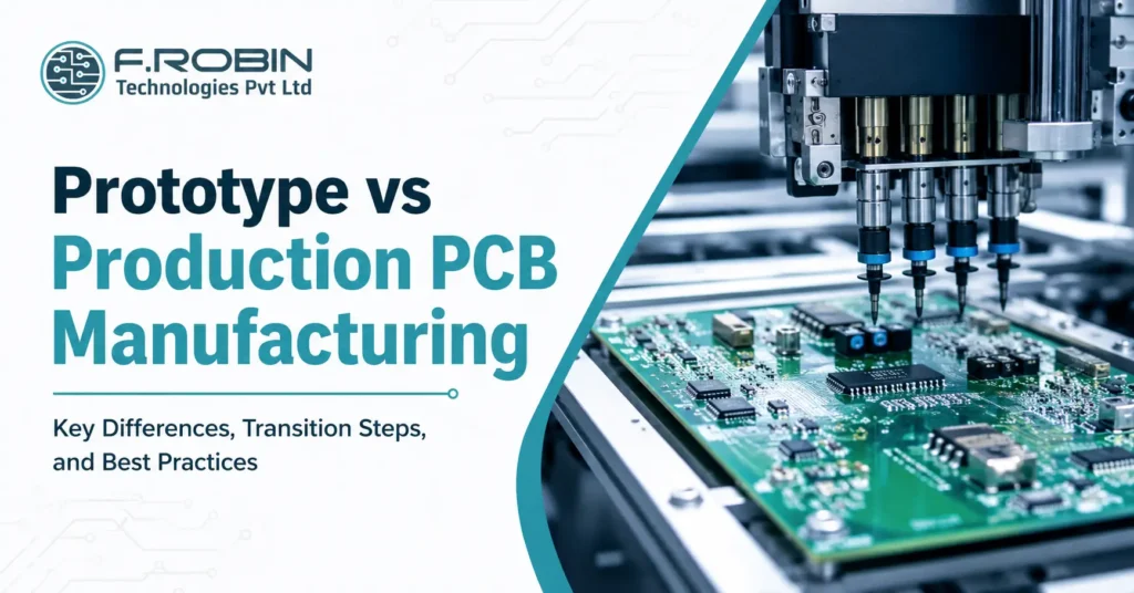
Circuit board manufacturing looks very different at the prototype stage than it does in full production. A prototype proves your design works; production proves you can build it reliably, affordably, and at scale. Confuse the two and you risk wasted money, delays, or a board that works in the lab but stumbles on the line. So what actually changes as you move from a handful of boards to thousands? In this guide, we compare prototype and production circuit board manufacturing across cost, lead time, testing, tooling, and yield. You will also learn how to transition smoothly between the two — and the mistakes that trip teams up when they scale. What Changes Between Prototype and Production? The short answer: the goal changes. Prototype circuit board manufacturing optimizes for speed and learning, while production optimizes for cost, consistency, and yield. As a result, almost every choice from quantity to testing shifts when you scale your circuit board manufacturing. In the prototype phase, you build a few boards quickly to validate the design. Mistakes are expected, and revisions are frequent. By contrast, production assumes the design is locked. Here the focus moves to repeatable quality, low cost per board, and high yield across thousands of units. Understanding this shift early saves money. A board designed only to “work once” rarely survives the demands of mass production, so smart teams plan for both stages from the start. For the underlying process itself, see our PCB manufacturing guide. This stage shift also changes who you talk to and what you measure. In prototyping, engineers chase functionality and iterate fast. In production circuit board manufacturing, operations and quality teams chase repeatability, tracking yield, defect rates, and cost per board on every run. Recognizing that the metrics themselves change helps you set the right expectations with your manufacturer at each stage. Prototype Circuit Board Manufacturing The prototype stage exists to answer one question: does the design work? Speed and flexibility matter most here, not cost per board. Typical traits of prototype circuit board production include: Because you are still learning, prototypes prioritize fast feedback over efficiency. The aim is to find and fix problems cheaply, before they multiply across thousands of units. The Pilot / Pre-Production Run Between prototype and full production sits the pilot run a small batch, often 50 to a few hundred boards, built on production-like processes. This bridge stage is easy to skip but valuable to keep. A pilot run verifies that your design is ready for volume. It exposes assembly issues, confirms test coverage, and reveals yield problems before you commit to a large order. Consequently, a good pilot prevents expensive surprises during mass production. Think of it as a dress rehearsal for the production line. So when are you ready to scale? You are ready when the design is stable across several prototypes, the pilot hits an acceptable yield, and your test coverage reliably catches real defects. Until those three boxes are ticked, moving to volume circuit board manufacturing only multiplies risk. Production Circuit Board Manufacturing Production circuit board manufacturing assumes the design is final and shifts the focus to scale. Now cost, consistency, and yield drive every circuit board manufacturing decision. Typical traits of production-stage printed circuit board production include: At this stage, small inefficiencies multiply. Therefore, production rewards careful design-for-manufacturing (DFM) and disciplined process control far more than the prototype stage ever did. Getting DFM right before this point is the single best lever for protecting yield at volume. Prototype vs Production: Side-by-Side This table summarizes how circuit board manufacturing changes across the two stages. Factor Prototype PCB Manufacturing Production PCB Manufacturing Quantity 1–50 boards Hundreds to thousands of boards Cost per Board High High Lead Time week Longer setup, fast throughput Automation Low priority Full automation Revisions Frequent design changes Design locked and validated Testing Basic and functional testing ICT, AOI, and comprehensive functional testing Yield Focus High priority priority Critical manufacturing metric Goal Validate the design Scale production reliably and cost-effectively Use this as a planning reference. The clearer you are about which stage you are in, the better your quotes and timelines will be. How to Transition From Prototype to Production Scaling up your circuit board manufacturing is a process, not a single leap. Follow these steps for a smooth transition: This staged approach reduces risk at every step. Moreover, qualifying your fab and assembly partner early ideally one that also offers PCB assembly avoids re-qualification later. Choosing the Right Partner for Each Stage Not every fab excels at both stages of circuit board manufacturing. Quick-turn shops shine at prototypes but may lack volume capacity, while large-volume houses can be slow and costly for a handful of boards. So match the partner to your stage — or choose one that does both well. For prototypes, prioritize speed, flexibility, and responsive support. For production, prioritize capacity, yield discipline, and competitive cost per board. A partner that handles prototype, pilot, and production circuit board manufacturing under one roof saves you from re-qualifying a new supplier mid-project, which protects both your timeline and your hard-won yield data. If you expect to scale, raise the question early. Ask prospective suppliers how they handle the jump from prototype to pcb board production, what their typical yields are at volume, and how they manage the pilot stage in between. Their answers quickly reveal whether they can grow with you. Common Mistakes When Scaling Up Teams often stumble at the prototype-to-production handoff. Watch for these: Avoiding these mistakes keeps your circuit board production reliable, profitable, and on schedule. Key Takeaways Conclusion Circuit board manufacturing is not one process but two mindsets. Prototyping chases speed and learning; production chases cost, consistency, and yield. The teams that scale smoothly plan for both from day one — locking the design, running a pilot, tightening test coverage, and qualifying their supplier before ramping volume. Ready to Take Your Board from Prototype to Production? Our PCB manufacturing services support everything from quick-turn prototypes to high-volume production
PCB Assembly Explained: SMT, THT and Mixed Builds
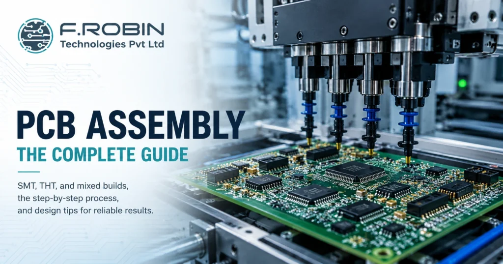
PCB assembly is the process that turns a bare board into a working electronic product by mounting and soldering components onto it. If you have ever wondered how a blank circuit board becomes the brain of a device, this guide explains it clearly. We cover the three main methods — SMT, THT, and mixed builds — along with the step-by-step process and how to prepare your design for clean results. Whether you are a hardware startup ordering your first build or an engineer comparing pcb assembly services, understanding these basics helps you avoid defects, control cost, and choose the right method. So let us break down exactly how it works, stage by stage. What Is PCB Assembly? PCB assembly, often called PCBA, is the process of soldering electronic components onto a bare printed circuit board to create a functional assembly. In short, the bare board provides the wiring, and assembly adds the parts that make the circuit work. This is different from board fabrication. Fabrication produces the empty board with its copper traces and layers, while the assembly of printed circuit boards populates that board with resistors, capacitors, ICs, connectors, and more. Both steps are essential, but they are distinct processes — often handled on different lines or even by different vendors. Modern assembly uses three approaches: surface-mount technology (SMT), through-hole technology (THT), and mixed builds that combine the two. The method you choose depends on your components, volume, and reliability needs. Next, let us compare them. SMT vs THT vs Mixed Builds The three assembly methods suit different parts and applications. Here is how each works. Surface-Mount Technology (SMT) SMT mounts components directly onto the surface of the board using solder paste and reflow soldering. Because SMT parts are small and need no leads through the board, they enable dense, compact designs. As a result, SMT dominates modern electronics and most high-volume pcb board assembly. Through-Hole Technology (THT) THT inserts component leads through drilled holes and solders them on the opposite side, usually with wave or selective soldering. THT joints are mechanically strong, so they suit connectors, large capacitors, and parts that face stress or heat. Consequently, THT remains valuable even in an SMT-first world. Mixed-Technology Builds Many boards need both. A mixed build uses SMT for the bulk of components and THT for connectors and high-stress parts. This combination is extremely common, though it adds process steps and therefore cost. Factor SMT THT Component Size Small, dense Larger, leaded Soldering Reflow Wave / Selective Mechanical Strength Moderate High Automation Fully automated Partly manual Best For High-volume, compact designs Connectors, high-stress parts Which Method Should You Use? In practice, the choice is rarely either-or. Use SMT wherever you can, because it is faster, cheaper at volume, and supports the smallest parts. Reach for THT only where you need it — for connectors, transformers, large electrolytic capacitors, and anything that takes mechanical or thermal stress. When a board needs both, accept the mixed build and plan the process order so SMT runs first and through-hole parts follow. Volume matters too. For a handful of prototypes, hand or selective soldering may be most economical. For thousands of units, fully automated SMT lines win on cost and consistency. Match the method to your parts and your production scale, and the decision usually makes itself. The PCB Assembly Process Step by Step Here is a typical SMT-led assembly flow, with the THT steps that follow. Each stage feeds the next, so a problem early on — such as poor solder paste — shows up as defects later. Therefore, process control at every step keeps yields high. Inspection and Quality Quality control runs throughout the build, not just at the end. Several methods verify a reliable assembly: Reputable pcb assembly services follow the IPC-A-610 standard for acceptability, which defines what a good solder joint and assembly look like. Asking which IPC class a provider works to is a quick way to gauge their quality discipline. How to Prepare Your Design for Assembly Good design makes assembly faster, cheaper, and more reliable — a practice called design for assembly (DFA). Apply these tips before you release your board: These steps connect directly to your layout work. For the full picture, see our guide to the printed circuit board design workflow, and confirm your stack-up and footprints during PCB layout design services. Common Assembly Defects and How to Avoid Them Even automated lines produce defects when the design or process slips. Watch for these: Most defects trace back to design or solder paste, so strong DFA and process control prevent the majority before they happen. Choosing a PCB Assembly Partner When you search for “pcb assembly near me” or compare providers, look beyond price. Confirm the partner offers the right method (SMT, THT, or mixed), follows IPC-A-610, performs AOI and electrical test, and handles your volume — from prototype to production. A local partner often eases communication and speeds up the build, while a turnkey provider that also handles PCB manufacturing and component sourcing can simplify your whole supply chain. Either way, a provider with strong quality discipline protects your product and your timeline. Decide too whether you want a turnkey build, where the partner sources every component, or a consigned build, where you supply the parts. Turnkey saves you procurement effort, while consigned gives you tighter control over sourcing — useful when you already hold stock or have allocation deals on key parts. Key Takeaways Conclusion PCB assembly is where a bare board becomes a real product. Whether you choose SMT for dense designs, THT for mechanical strength, or a mixed build for both, the process follows a clear path — paste, place, reflow, inspect, insert, and test. Above all, strong design for assembly and solid quality control keep your boards reliable and your costs predictable. Ready to Build Your Boards? Our turnkey PCB manufacturing and assembly services cover SMT, THT, and mixed-technology builds with IPC-compliant quality from prototype to volume production. Talk to
Types of PCB Manufacturing Process: A Complete Guide for Engineers and Buyers
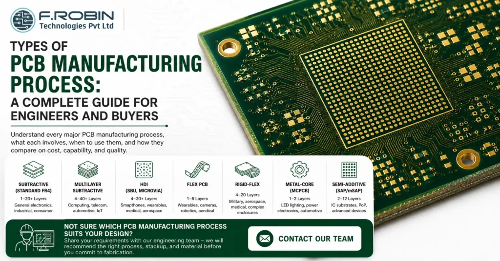
Introduction The types of PCB manufacturing process determine everything downstream board complexity, layer count, material choice, cost, lead time, and the electrical performance of the finished board. Yet for most hardware teams, the manufacturing process is a black box: you send Gerbers, you receive boards. Understanding what actually happens inside that black box — and which process applies to which board type helps you make better design decisions, write more accurate specifications, choose the right fabricator, and avoid costly surprises at the DFM stage. In this guide, we cover every major PCB manufacturing process type, what each involves, when each is appropriate, and how they compare on cost, capability, and quality. 1. The Core PCB Manufacturing Process Subtractive Fabrication The most widely used PCB manufacturing process globally is subtractive fabrication also called the subtractive method or print-and-etch process. It is the standard process for the vast majority of FR4 rigid PCBs manufactured today, from single-layer boards to complex multilayer designs. How the subtractive process works The subtractive process starts with a copper-clad laminate a fibreglass substrate (FR4) with copper foil bonded to one or both sides. The unwanted copper is selectively removed through a sequence of imaging, etching, and plating steps, leaving behind only the copper traces, pads, and planes defined by the design. Preparing the Inner Layers Step 1 — Photolithography (inner layer imaging) The copper surface is coated with a light-sensitive photoresist. A photomask or in modern facilities, a laser direct imaging (LDI) system exposes the circuit pattern onto the resist. Consequently, the unexposed resist is washed away, and the exposed copper underneath is chemically etched off. What remains is precisely the copper circuit pattern of that layer. Step 2 — Lamination For multilayer boards, the individual inner layers are stacked with prepreg (glass-fibre epoxy resin sheets) between them and bonded under heat and pressure in a hydraulic lamination press. As a result, all layers fuse into a single rigid, uniform substrate. Step 3 — Mechanical and laser drilling CNC drilling machines create holes for through-hole component leads, via connections between copper layers, and mechanical mounting points. In addition, high-density boards use laser drilling to create microvias holes too small for mechanical drills, typically under 150µm in diameter. Finishing the Board Step 4 — Through-hole plating The drilled holes are copper-plated by electroless deposition followed by electrolytic plating, creating a conductive copper barrel through the hole that electrically connects layers. This step is fundamentally what distinguishes a multilayer PCB from a simple stack of copper sheets. Step 5 — Outer layer imaging and etching Following plating, the outer copper layers go through the same photolithography and etching process as the inner layers, defining the surface traces, pads, and planes. Step 6 — Solder mask, surface finish, and silkscreen A liquid photoimageable solder mask (LPI) is applied and cured, opening only the pad areas. A surface finish (HASL, ENIG, OSP, or hard gold) is applied to exposed pads. Finally, reference designators and component outlines are printed as silkscreen. Step 7 — Electrical test and delivery Every board is electrically tested by flying probe or bed of nails before shipment, verifying continuity and absence of shorts. The subtractive process is cost-effective, mature, and supported by every PCB fabricator in India and globally. For standard FR4 rigid boards — single layer through to 20+ layers it remains the default manufacturing method. 2. Multilayer PCB Manufacturing Process Multilayer PCB manufacturing follows the same subtractive process as single and double-sided boards, but adds repeated lamination cycles to build up the layer stack. It is the dominant process for all complex, high-density electronic designs. What makes multilayer manufacturing different Layer count options Multilayer boards are built in even numbers of layers: 4, 6, 8, 10, 12, and up to 40+ layers for advanced computing and telecommunications hardware. Each additional pair of layers adds one lamination cycle, drilling pass, and plating step. Inner Layer Processing Core fabrication Each inner layer starts as a separate copper-clad core a rigid substrate with copper on both sides. The circuit pattern is imaged and etched onto each core individually before the stack is assembled. Crucially, inner layers cannot be reworked after lamination, so imaging yield at this stage must be near-perfect. Prepreg and stackup Between each core, sheets of prepreg (B-stage epoxy glass) are placed. The stackup sequence which layers are signal, power, or ground is defined by the designer and must be communicated to the fabricator in the stackup specification. Signal integrity, controlled impedance, and EMI performance all depend on correct stackup execution. Via Types in Multilayer Boards Through-hole vias pass from the top surface to the bottom surface through all layers. They are drilled after lamination and plated in a single pass the most common and least expensive via type. Blind vias connect an outer layer to one or more inner layers without passing all the way through the board. They require sequential lamination laminating a partial stack, drilling and plating, then laminating further layers on top. Buried vias connect two or more inner layers without reaching either outer surface. They are drilled and plated before lamination and are invisible in the finished board. Microvias are laser-drilled vias with diameters typically below 150µm, used in HDI (High-Density Interconnect) designs. They enable very high component density by connecting adjacent layers over a very short distance. Multilayer PCB manufacturing requires tighter process control than single or double-sided boards because registration errors between layers compound with each added layer. For a 12-layer board, the inner layer alignment tolerance must be held across 10 separate imaging and etching cycles. 3. HDI PCB Manufacturing Process (High-Density Interconnect) HDI PCB manufacturing is a specialised extension of multilayer fabrication designed for boards with extremely high component density smartphones, wearables, advanced IoT modules, medical implants, and aerospace electronics. What defines HDI manufacturing HDI boards are characterised by line widths and spaces below 100µm, via diameters below 150µm (microvias), via-in-pad structures, and sequential build-up (SBU) lamination. As a result, they achieve far greater routing density
PCB Fabrication vs PCB Assembly: What’s the Difference and Why It Matters
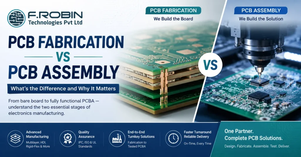
Introduction PCB fabrication vs PCB assembly these two terms appear constantly in electronics manufacturing, often interchangeably and almost always incorrectly. If you have ever sent a quote request to a manufacturer and been unsure whether to ask for “fabrication,” “assembly,” or both, this guide will clear that up completely. In short: fabrication makes the board, while assembly populates it. Together, they produce a functional PCBA. However, the details of each process the different expertise they require, the distinct quality standards they are held to, and the cost implications of each are worth understanding in full, especially if you are about to place your first manufacturing order or are evaluating new suppliers. 1. What Is PCB Fabrication? PCB fabrication is the process of manufacturing the bare printed circuit board — the physical substrate with copper traces, drilled holes, plated vias, solder mask, and silkscreen — but with no components attached. Think of it as building the foundation of a building before any furniture goes in. The board comes out of fabrication as a flat, component-free physical object that carries the electrical connectivity your design requires. Every trace, pad, via, and plane is in place, yet nothing is soldered and nothing is placed. What Happens During PCB Fabrication Preparing the Inner Layers Step 1 — Inner layer imaging (multilayer boards) Copper-clad laminate sheets are coated with photoresist. Next, UV light exposes the circuit pattern onto the resist through a film or laser direct imaging (LDI) system. Unexposed resist is then washed away, and the exposed copper is etched off — leaving only the copper traces of that layer. Step 2 — Lamination For multilayer boards, the individual inner layers are stacked with prepreg (glass-fibre resin sheets) between them and pressed together under heat and pressure in a lamination press. As a result, all layers bond into a single rigid substrate. Step 3 — Drilling CNC drilling machines drill holes through the laminated stack for through-hole component leads, via connections between layers, and mechanical mounting holes. In addition, high-density boards may use laser drilling for microvias where standard CNC cannot reach the required diameter. Step 4 — Plating The drilled holes are electrolessly copper-plated to create electrical conductivity between layers. This plating step is precisely what makes a via a via — a copper-plated barrel connecting two or more copper layers through a drilled hole. Finishing the Board Surface Step 5 — Outer layer imaging and etching Following inner layer processing, the outer copper layers go through the same imaging and etching process, defining the surface traces and pads. Step 6 — Solder mask application A liquid photoimageable solder mask (LPI) is applied over the entire board surface, then exposed and developed to open only the pad areas. Consequently, the traces remain protected by the green (or black, red, or blue) coating you see on a finished PCB, which prevents solder bridging during assembly and protects copper from oxidation. Step 7 — Surface finish The exposed copper pads receive a surface finish to prevent oxidation and ensure good solderability. Common finishes include: Step 8 — Silkscreen printing Reference designators, component outlines, polarity markers, logos, and other markings are printed on the board using white or yellow ink. This silkscreen layer is what your assembler and operators use as a visual reference during assembly and inspection. Step 9 — Electrical testing Every fabricated board is electrically tested — either by flying probe or bed of nails — to verify that all nets are continuous and no unintended shorts exist. Importantly, a board that fails electrical test at fabrication never reaches assembly. Step 10 — Visual inspection, routing, and delivery Finally, boards are inspected visually and under AOI, then routed from the production panel into individual boards or arrays and packaged for delivery. 2. What Is PCB Assembly? PCB assembly (PCBA) is the process of soldering electronic components onto the fabricated bare board to create a functional electronic circuit. Whereas fabrication builds the substrate, assembly populates it. The assembled board — called a PCBA (Printed Circuit Board Assembly) — is the finished functional unit: the thing that goes into your product, gets tested, and performs the electronic function your design was created for. What Happens During PCB Assembly Step 1 — Solder paste stencil printing A laser-cut stainless steel stencil is aligned over the bare board. Solder paste is then squeegeed across the stencil, depositing precise volumes of paste only on the pad areas through the stencil apertures. Critically, paste volume and consistency at this step directly determines solder joint quality downstream. Step 2 — SMT component placement (pick and place) An automated pick-and-place machine retrieves components from reels, trays, and tubes, then places them on the solder-pasted pads with micron-level accuracy. Modern machines handle components as small as 0201 (0.6mm × 0.3mm) and manage fine-pitch BGAs, QFNs, and multi-pin connectors in the same pass. Step 3 — Reflow soldering The populated board travels through a multi-zone reflow oven on a conveyor. Throughout this stage, the temperature profile — preheat, thermal soak, reflow peak, and cooling — is precisely controlled to melt and resolidify the solder paste into reliable intermetallic solder joints without damaging components. Profiles are customised per board based on component thermal sensitivity and paste specification. Step 4: Removed “through-hole components” → replaced with “components” (the step heading already tells the reader it’s through-hole) Step 5: Replaced “Through-hole component leads on the bottom of the board are subsequently soldered” → replaced with “Once insertion is complete, the leads on the bottom of the board are soldered” — breaks the consecutive pattern and adds a transition word Yoast will also count Step 6 — Inspection AOI (Automated Optical Inspection) scans every board for missing components, wrong orientation, solder bridges, lifted leads, and insufficient solder. Additionally, X-ray inspection checks hidden solder joints on BGA and QFN packages, while visual inspection by trained operators provides a final check. Step 7 — Testing Electrical testing (flying probe or ICT) verifies circuit continuity and component values. Furthermore,
SMT vs Through-Hole Assembly: Which Soldering Method Is Right for Your PCB?
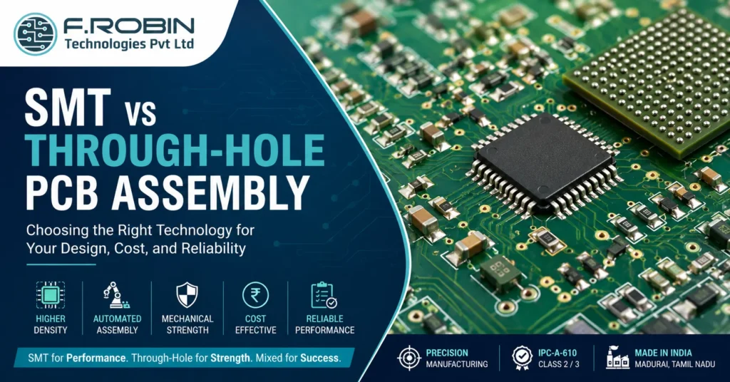
Introduction When it comes to SMT vs through-hole assembly, choosing the wrong method for your PCB can quietly inflate your manufacturing cost, delay your timeline, and create reliability problems that only surface after your product ships. Every PCB design reaches a moment where the engineer has to decide: surface mount, through-hole, or both? It sounds like a technical detail, but it directly affects your assembly cost, board size, mechanical reliability, and how quickly you can get boards back from your manufacturer. This guide breaks down both methods clearly — what they are, where each one wins, and how to make the right choice for your specific application. Whether you are designing a compact IoT sensor, a ruggedised industrial controller, or a power electronics board, understanding SMT vs through-hole assembly is a decision that matters more than most teams realise. 1. What Is SMT (Surface Mount Technology)? Surface mount technology places components directly onto the surface of the PCB. Components have no leads that pass through the board — instead they have flat pads or small solder balls that sit on copper pads on the top or bottom surface, held in place by solder paste and reflowed in an oven. Common SMT component packages The smallest SMT passives in common use today — 01005 (0.4mm × 0.2mm) — are about the size of a grain of sand. BGA packages hide hundreds of solder balls underneath the IC body in a grid matrix, requiring X-ray inspection to verify assembly quality. SMT is the dominant assembly technology for virtually all modern consumer electronics, IoT devices, smartphones, and computing hardware. 2. What Is Through-Hole Assembly? Through-hole assembly uses components with wire leads that pass through drilled holes in the PCB. The leads are soldered on the opposite side of the board — either by wave soldering, selective soldering, or hand soldering. Through-hole was the dominant PCB assembly method from the 1950s through the late 1980s. Today it is used selectively, primarily for components where mechanical strength, high current capacity, or replaceability matter more than board density. Common through-hole component packages Through-hole components are still the right choice for connectors that will be plugged and unplugged repeatedly, high-voltage or high-current components, and components that must survive mechanical vibration or shock. 3. Key Differences — Board Density, Mechanical Strength, Cost, Speed Here is how the two technologies compare across the metrics that matter most in production decisions: Factor SMT Through-hole Board Density Very high — components on both sides, no drill holes required Low — holes reduce routing space; components typically one side only Component Size Extremely small (down to 0.4mm × 0.2mm) Larger — requires lead pitch and hole clearance Mechanical Strength Moderate — relies on solder joint to PCB surface High — lead passes through board and is soldered on both sides Assembly Speed Very fast — automated pick and place at 20,000–60,000 cph Slower — insertion requires machines or manual operators Assembly Cost (Volume) Low at high volume — fully automated Higher — manual or semi-automated insertion adds labour Prototype Cost Moderate — stencil and setup NRE Lower for hand-soldered prototypes Rework / Repair Harder — requires hot air, tweezers, fine-pitch tools Easier — leads can be clipped, reflowed, replaced with standard tools Vibration Resistance Lower Higher — lead-through-hole provides mechanical anchor 4. When to Use SMT Choose SMT as your primary assembly method when: You need small form factor. SMT components are 10–100× smaller than their through-hole equivalents. A 0402 resistor is 1.0mm × 0.5mm. The SMD equivalent of a 16-pin DIP IC might be a QFN at 3mm × 3mm. If your board needs to fit inside a compact enclosure, SMT is not optional — it is the only viable path. You are designing for high-volume production. Automated SMT lines can place and solder thousands of components per hour with minimal human intervention. Unit cost drops sharply at volume because the machine cost is amortised across a large number of builds. Pick-and-place machines handle component placement; reflow ovens handle soldering — no manual intervention required. You are building IoT or consumer electronics. Virtually all IoT modules, Bluetooth chips, Wi-Fi SoCs, microcontrollers, and sensors are only available in SMT packages. If your BOM includes an ESP32, nRF52, STM32, or similar, you are already committed to SMT. You want double-sided assembly. SMT components can be placed and reflowed on both sides of the board, dramatically increasing routing and component density without increasing board size. You need controlled impedance or high-frequency routing. Drill holes in through-hole designs create via stubs and discontinuities in signal paths. All-SMT designs with controlled via placement offer much better signal integrity for RF, high-speed digital, and power switching applications. 5. When to Use Through-Hole Through-hole is the right choice — even in predominantly SMT designs — for specific component types: High-stress connectors. USB ports, D-sub connectors, RJ45 jacks, and power barrel jacks that are plugged and unplugged repeatedly put mechanical stress on the solder joint. Through-hole soldering anchors the connector mechanically through the board rather than relying only on surface adhesion. For consumer products with daily use, through-hole connectors last significantly longer. Power components. Large electrolytic capacitors (≥100µF, 25V+), wirewound resistors, high-current inductors, and power transistors in TO-220 or TO-247 packages all exist in through-hole form for good reason — they handle heat and current that would stress smaller SMD packages. Heat sinking through the lead and board is also more effective. High-vibration environments. Automotive electronics, industrial machinery, robotics, and aerospace applications expose boards to continuous mechanical vibration. Through-hole components, with their leads soldered on both board sides, resist mechanical loosening far better than SMT joints under sustained vibration. Prototyping with socketed ICs. Through-hole DIP ICs can be socketed — inserted into ZIF (Zero Insertion Force) or DIP sockets — allowing you to swap microcontrollers, EEPROMs, or op-amps during development without soldering and desoldering repeatedly. For R&D boards where component swaps are expected, this is invaluable. High-voltage isolation. Safety-critical applications requiring specific creepage and clearance distances between high-voltage
Turnkey PCB Assembly Services in India: Everything You Need to Know Before Placing an Order
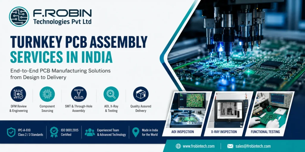
Introduction Turnkey PCB assembly services India are becoming essential for hardware startups, OEMs, R&D teams, and electronics companies looking for reliable PCB manufacturing, component sourcing, SMT assembly, testing, and fast production support under one roof. Whether you are building a prototype, pilot batch, or full production run, choosing the right turnkey PCB assembly partner directly affects product quality, lead times, and manufacturing cost. So you have a PCB design ready. The Gerbers are exported, the BOM is drafted, and you need someone to build it. You search for PCB assembly services in India and are immediately confronted with unfamiliar terms like turnkey, partial turnkey, consignment, PCBA, SMT, AOI, and functional testing. This guide explains everything you need to know before placing an order for turnkey PCB assembly services in India, including the assembly process, testing methods, file preparation, pricing factors, and how to choose the right EMS manufacturing partner. 1. What Are Turnkey PCB Assembly Services in India? Turnkey PCB assembly means you hand off the job completely — design files, BOM, and sometimes the bare PCBs — and receive assembled, tested boards in return. The manufacturer handles component sourcing, procurement, kitting, solder paste printing, pick-and-place, reflow, inspection, and often functional testing. The Three Models Full Turnkey You supply only design files (Gerbers, BOM, centroid file). The manufacturer procures all components, fabricates bare boards, assembles, inspects, and ships finished boards. The most hands-off and most popular option for startups and hardware teams without procurement infrastructure. Partial Turnkey (Kitted Assembly) You supply some components — long-lead items or proprietary parts — and the manufacturer supplies the rest. Common for products with custom ICs, specialised sensors, or parts under NDA. Consignment (CM-Only) You supply everything: bare boards, all components, stencil, sometimes solder paste. The manufacturer provides only assembly labour and equipment. Used by large OEMs with established supply chains. 2. The Turnkey PCBA Process End to End 3. SMT vs Through-Hole Assembly in the Turnkey Context Most modern PCBs are predominantly SMT, but boards with both SMT and through-hole components require understanding the two-pass process. Pure SMT boards are the fastest and most cost-effective to assemble. The entire process is automated. If your design can be fully SMT — using SMD connectors, SMD electrolytic capacitors, SMD crystals — do it. Mixed technology boards (SMT + through-hole) require two passes: SMT components are placed and reflowed first; through-hole components are then inserted and selectively soldered. This adds time and cost, but is often unavoidable for high-current power components and ruggedised connectors. Pure through-hole boards are rare today and are assembled by hand insertion and wave soldering. 4. AOI, X-Ray, and Functional Testing in Turnkey Lines Testing is where many low-cost assemblers cut corners — and where you pay the price when field failures occur. Automated Optical Inspection (AOI) AOI machines use high-resolution cameras and image processing to inspect every solder joint and component placement. AOI catches: What AOI misses: Hidden solder joints (BGA balls, QFN thermal pads), electrical opens/shorts that don’t show optically, and functional failures. X-Ray Inspection X-ray is essential for BGA, QFN, and LGA packages where solder joints are hidden under the component body. It reveals: For any board with a BGA or QFN component, X-ray inspection is mandatory, not optional. In-Circuit Testing (ICT) ICT uses a “bed of nails” fixture with spring-loaded probes contacting test points to measure component values and check for shorts/opens. Fast and thorough but requires a custom fixture costing ₹50,000–₹3,00,000+. Economical only at 500+ units. Flying Probe Testing Flying probe uses movable probes without a custom fixture — ideal for prototype and low-volume runs. Slower than ICT but fixture-free and catches shorts, opens, and component value errors. Functional Testing (FCT) FCT powers up the assembled board and exercises it exactly as in the final product. A custom test jig interfaces with the board’s connectors and I/O, stimulates inputs, and measures outputs. FCT is the only test method that definitively proves the board works. Recommended Testing Strategy by Volume Production Volume Recommended Tests 1–10 Units (Prototype) Visual Inspection + Flying Probe Testing + Functional Circuit Testing (FCT) 10–100 Units (Pilot Run) AOI + X-ray Inspection (for BGA/QFN) + Functional Circuit Testing (FCT) 100–1,000 Units AOI + X-ray Inspection + ICT or Flying Probe Testing + Functional Circuit Testing (FCT) 1,000+ Units (Mass Production) AOI + X-ray Inspection + ICT + Functional Circuit Testing (FCT) + Burn-In Testing 5. Component Sourcing in India — Counterfeit Risk, and Approved Vendor Lists Component sourcing is one of the most overlooked aspects of turnkey assembly — and one of the most consequential. Counterfeit Component Risk Counterfeit electronic components are a real problem, especially sourced through grey-market channels. Counterfeits can fail immediately, pass initial testing and fail in the field, or cause safety issues. To mitigate risk: Approved Vendor Lists (AVL) An AVL is a list of approved manufacturers and distributors for each BOM line item. For prototype runs, authorised distributors are sufficient. For production, define and submit your AVL with your production BOM. 6. How to Prepare Files for Turnkey Assembly Poor file preparation is the single most common cause of delays, miscommunications, and assembly errors. Gerber Files (RS-274X Format) Include: all copper layers, solder mask layers (top and bottom), silkscreen layers, drill file (Excellon format), and board outline. Name layers clearly. Double-check: Bill of Materials (BOM) Every component must include: A BOM with only generic descriptions (“100nF capacitor, 0402”) forces sourcing assumptions that may not match your design intent. Always provide MPNs. Centroid / Pick-and-Place / XY File Contains reference designator, X and Y coordinates, rotation angle, and board side for every SMT component. Export from your PCB tool and verify the coordinate origin matches your Gerber origin. A mismatch causes your assembler to manually adjust every component location. Assembly Drawing A 2D PDF showing top and bottom of the assembled board with reference designators visible, polarity markings for diodes and electrolytic capacitors, and any special assembly notes. Test Specification (for FCT) Describe what the board must do, how
