
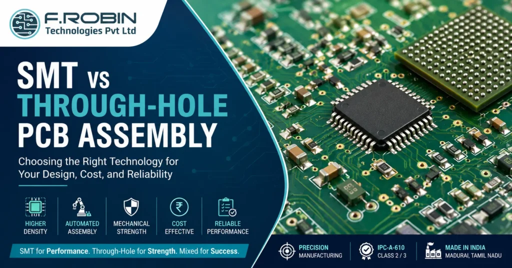
Introduction
When it comes to SMT vs through-hole assembly, choosing the wrong method for your PCB can quietly inflate your manufacturing cost, delay your timeline, and create reliability problems that only surface after your product ships.
Every PCB design reaches a moment where the engineer has to decide: surface mount, through-hole, or both? It sounds like a technical detail, but it directly affects your assembly cost, board size, mechanical reliability, and how quickly you can get boards back from your manufacturer.
This guide breaks down both methods clearly — what they are, where each one wins, and how to make the right choice for your specific application. Whether you are designing a compact IoT sensor, a ruggedised industrial controller, or a power electronics board, understanding SMT vs through-hole assembly is a decision that matters more than most teams realise.
1. What Is SMT (Surface Mount Technology)?
Surface mount technology places components directly onto the surface of the PCB. Components have no leads that pass through the board — instead they have flat pads or small solder balls that sit on copper pads on the top or bottom surface, held in place by solder paste and reflowed in an oven.
Common SMT component packages
- Passive components: 0402, 0603, 0805 resistors and capacitors (sizes in inches × 100, e.g. 0402 = 0.04″ × 0.02″)
- ICs: SOIC, QFP, QFN, BGA, LGA, CSP
- Transistors and diodes: SOT-23, SOD-123
- Connectors: SMD headers and USB connectors
The smallest SMT passives in common use today — 01005 (0.4mm × 0.2mm) — are about the size of a grain of sand. BGA packages hide hundreds of solder balls underneath the IC body in a grid matrix, requiring X-ray inspection to verify assembly quality.
SMT is the dominant assembly technology for virtually all modern consumer electronics, IoT devices, smartphones, and computing hardware.
2. What Is Through-Hole Assembly?
Through-hole assembly uses components with wire leads that pass through drilled holes in the PCB. The leads are soldered on the opposite side of the board — either by wave soldering, selective soldering, or hand soldering.
Through-hole was the dominant PCB assembly method from the 1950s through the late 1980s. Today it is used selectively, primarily for components where mechanical strength, high current capacity, or replaceability matter more than board density.
Common through-hole component packages
- ICs: DIP (Dual In-line Package) — 8, 14, 16, 28, 40-pin
- Connectors: D-sub, DB9, USB-B, terminal blocks, edge connectors
- Passive components: Large electrolytic capacitors, wirewound resistors, inductors
- Switches, relays, fuses: Panel-mount and PCB-mount varieties
- Power components: Transformers, high-current MOSFETs in TO-220 package
Through-hole components are still the right choice for connectors that will be plugged and unplugged repeatedly, high-voltage or high-current components, and components that must survive mechanical vibration or shock.
3. Key Differences — Board Density, Mechanical Strength, Cost, Speed
Here is how the two technologies compare across the metrics that matter most in production decisions:
| Factor | SMT | Through-hole |
|---|---|---|
| Board Density | Very high — components on both sides, no drill holes required | Low — holes reduce routing space; components typically one side only |
| Component Size | Extremely small (down to 0.4mm × 0.2mm) | Larger — requires lead pitch and hole clearance |
| Mechanical Strength | Moderate — relies on solder joint to PCB surface | High — lead passes through board and is soldered on both sides |
| Assembly Speed | Very fast — automated pick and place at 20,000–60,000 cph | Slower — insertion requires machines or manual operators |
| Assembly Cost (Volume) | Low at high volume — fully automated | Higher — manual or semi-automated insertion adds labour |
| Prototype Cost | Moderate — stencil and setup NRE | Lower for hand-soldered prototypes |
| Rework / Repair | Harder — requires hot air, tweezers, fine-pitch tools | Easier — leads can be clipped, reflowed, replaced with standard tools |
| Vibration Resistance | Lower | Higher — lead-through-hole provides mechanical anchor |
4. When to Use SMT
Choose SMT as your primary assembly method when:
You need small form factor. SMT components are 10–100× smaller than their through-hole equivalents. A 0402 resistor is 1.0mm × 0.5mm. The SMD equivalent of a 16-pin DIP IC might be a QFN at 3mm × 3mm. If your board needs to fit inside a compact enclosure, SMT is not optional — it is the only viable path.
You are designing for high-volume production. Automated SMT lines can place and solder thousands of components per hour with minimal human intervention. Unit cost drops sharply at volume because the machine cost is amortised across a large number of builds. Pick-and-place machines handle component placement; reflow ovens handle soldering — no manual intervention required.
You are building IoT or consumer electronics. Virtually all IoT modules, Bluetooth chips, Wi-Fi SoCs, microcontrollers, and sensors are only available in SMT packages. If your BOM includes an ESP32, nRF52, STM32, or similar, you are already committed to SMT.
You want double-sided assembly. SMT components can be placed and reflowed on both sides of the board, dramatically increasing routing and component density without increasing board size.
You need controlled impedance or high-frequency routing. Drill holes in through-hole designs create via stubs and discontinuities in signal paths. All-SMT designs with controlled via placement offer much better signal integrity for RF, high-speed digital, and power switching applications.
5. When to Use Through-Hole
Through-hole is the right choice — even in predominantly SMT designs — for specific component types:
High-stress connectors. USB ports, D-sub connectors, RJ45 jacks, and power barrel jacks that are plugged and unplugged repeatedly put mechanical stress on the solder joint. Through-hole soldering anchors the connector mechanically through the board rather than relying only on surface adhesion. For consumer products with daily use, through-hole connectors last significantly longer.
Power components. Large electrolytic capacitors (≥100µF, 25V+), wirewound resistors, high-current inductors, and power transistors in TO-220 or TO-247 packages all exist in through-hole form for good reason — they handle heat and current that would stress smaller SMD packages. Heat sinking through the lead and board is also more effective.
High-vibration environments. Automotive electronics, industrial machinery, robotics, and aerospace applications expose boards to continuous mechanical vibration. Through-hole components, with their leads soldered on both board sides, resist mechanical loosening far better than SMT joints under sustained vibration.
Prototyping with socketed ICs. Through-hole DIP ICs can be socketed — inserted into ZIF (Zero Insertion Force) or DIP sockets — allowing you to swap microcontrollers, EEPROMs, or op-amps during development without soldering and desoldering repeatedly. For R&D boards where component swaps are expected, this is invaluable.
High-voltage isolation. Safety-critical applications requiring specific creepage and clearance distances between high-voltage and low-voltage circuits are easier to manage with through-hole components, where lead pitch and hole spacing are larger and easier to control.
6. Mixed Technology Boards — Combining SMT and THT
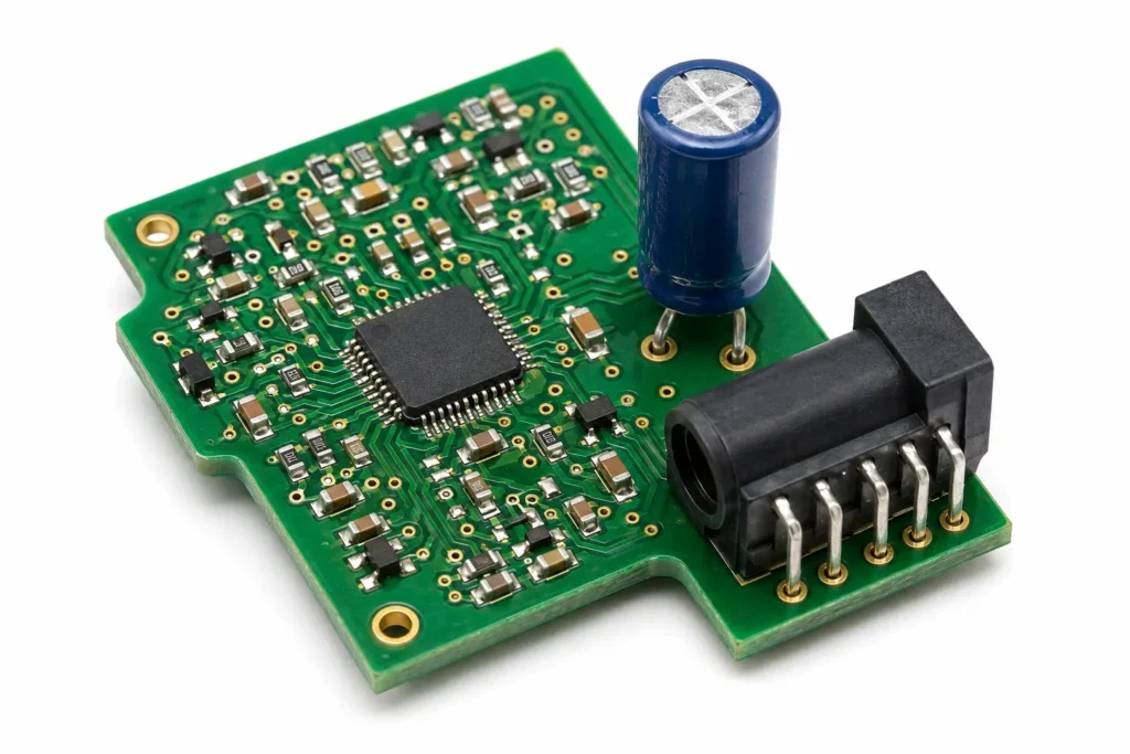
The reality is that most production boards use both technologies. The digital and analogue circuitry — ICs, passives, sensors — is SMT. The connectors, power components, and ruggedised parts are through-hole. This is called a mixed technology board and requires a specific assembly sequence:
Standard mixed assembly sequence:
- SMT solder paste printed on top side
- Top-side SMT components placed by pick-and-place
- Reflow oven — top-side SMT soldered
- Board flipped. SMT paste printed on bottom side (if double-sided SMT)
- Bottom-side SMT components placed
- Reflow oven — bottom-side SMT soldered
- Through-hole components hand-inserted or machine-inserted
- Selective soldering or wave soldering — through-hole components soldered
Important design consideration: Through-hole component leads on the bottom of the board must not be so close to bottom-side SMT components that wave or selective soldering damages them. Your PCB designer needs to ensure adequate keepout zones around bottom-side SMD components near through-hole areas.
Cost implication: Every additional assembly pass (second reflow, selective solder) adds time and cost. Minimise through-hole components on your BOM wherever possible. SMD connectors, SMD electrolytic caps, and SMD transformers have improved significantly and are viable replacements for through-hole equivalents in many non-ruggedised applications.
For F.Robin Technologies’ full PCB manufacturing capabilities — including mixed technology assembly, IPC-A-610 Class 2 and Class 3 workmanship, and AOI inspection — visit the PCB manufacturing services page.
7. Decision Guide
Use this to determine the right approach for your project:
Answer these four questions:
- Does your design include any standard through-hole-only components (large connectors, power transformers, panel-mount components)? → If yes: mixed technology is required regardless of other factors.
- Is your board smaller than 50mm × 50mm, or are you severely space-constrained? → If yes: SMT only. Through-hole takes too much space.
- Will the board experience continuous mechanical vibration, or will connectors be plugged/unplugged more than 500 times in product life? → If yes: use through-hole for those specific components.
- Is your volume above 100 boards? → If yes: optimise aggressively for SMT. Every through-hole component adds meaningful labour cost at scale.
The most common answer for modern electronic products is: primarily SMT, with through-hole reserved for connectors and power components. This gives you the density and automation benefits of SMT where it matters, and the mechanical robustness of through-hole where connectors and power components demand it.
Conclusion
SMT and through-hole are not competing technologies — they are complementary tools. SMT gives you density, speed, and automation at volume. Through-hole gives you mechanical strength and robustness where the application demands it. The best-designed boards use each method where it is genuinely the right choice, not as a default.
If you are designing a new board and are unsure which approach suits your application, F.Robin Technologies’ engineering team can review your schematic and BOM and advise on assembly method before you commit to a layout. We manufacture PCBs across the full spectrum — SMT, through-hole, and mixed technology — from our facility in Madurai, Tamil Nadu, held to IPC-A-610 Class 2/3 standards.
Learn more about our capabilities: PCB Manufacturing Services →
Not Sure Which Assembly Method Is Right for You?
Share your design with our team — we will review your BOM and schematic and recommend the right approach before you commit to a layout.
Contact Our Team