
When Do You Need FEA in Ansys vs Hand Calculations?
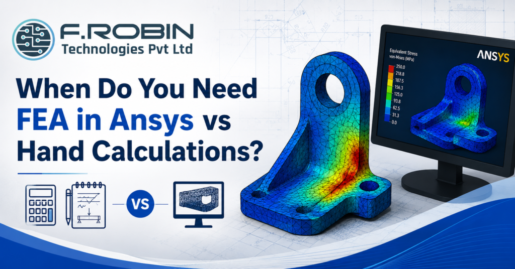
Every mechanical engineer faces the same question during structural analysis: do I reach for a quick hand calculation, or do I build a full FEA model in Ansys? Both are valid tools, and choosing the wrong one wastes time either by over-analyzing a simple part or by under-analyzing a complex one. The trick is knowing which method fits the problem in front of you. This decision guide answers exactly that. We compare hand calculations and FEA in Ansys across accuracy, complexity, cost, and time, then give you clear rules for when each is the right choice. Whether you are sizing a simple bracket or validating a vibration-critical assembly, you will know which structural analysis method to trust. What Is Structural Analysis? Structural analysis is the process of determining how a part or assembly responds to loads — the stresses, deflections, and safety margins it experiences in service. Its goal is simple: confirm that a design will not fail under the forces it must withstand. There are two broad ways to perform structural analysis. Hand calculations use established formulas and engineering theory to estimate stress and deflection quickly. Finite element analysis (FEA), run in tools like Ansys, divides a model into thousands of small elements and solves the physics numerically for complex shapes and loads. Neither method is universally better. Each suits different problems, and skilled engineers move fluidly between them. Knowing when to use which is the essence of efficient structural analysis. Hand Calculations: Strengths and Limits Hand calculations are fast, cheap, and transparent. Using standard beam, plate, and stress formulas, an engineer can size a part or check a load case in minutes — with full visibility into every assumption. Their strengths are speed and insight. Because you see the equations, you understand exactly what drives the result, which builds engineering intuition. They are ideal for simple geometry, standard load cases, and quick sanity checks. Their limits appear with complexity. Hand calculations struggle with intricate geometry, complex or combined loading, contact, and dynamic effects. For those, the simplifying assumptions break down, and you need a numerical method instead. FEA in Ansys: Strengths and Limits FEA in Ansys handles what hand calculations cannot. By meshing a model into small elements, it computes stress and deflection across complex 3D geometry, combined loads, contact, vibration, and nonlinear behaviour — cases with no clean closed-form solution. Its strength is versatility and detail. FEA reveals stress concentrations, mode shapes, and thermal effects that formulas miss, and it supports design optimization. For structural and vibration analysis of real assemblies, it is often the only practical option. The trade-offs are time, cost, and skill. FEA takes longer to set up, demands expertise, and — critically — can produce confident-looking but wrong answers if the mesh, boundary conditions, or material data are poor. Powerful as it is, FEA still needs judgement to trust. When Hand Calculations Are Enough Reach for hand calculations first when the problem is simple. In many cases, they give you the answer faster and with more insight than a full model would. Use them when: For a large share of everyday structural analysis, hand calculations are entirely sufficient. Jumping straight to FEA for a simple bracket wastes hours you could spend elsewhere. Match the effort to the problem. When You Need FEA in Ansys Turn to FEA in Ansys when complexity exceeds what formulas can handle. It becomes the right choice when: In these situations, a hand calculation cannot capture the real behaviour, and FEA earns its cost. Structural and vibration analysis of a full assembly, for example, almost always requires simulation. When failure is expensive or dangerous, the investment in FEA is clearly justified. Hand Calc vs FEA Comparison The table below compares the two methods at a glance. Factor Hand Calculations FEA in Ansys Speed Fast Slower to set up Cost Low Higher Geometry Simple shapes Complex 3D models Loads Standard loading conditions Combined, dynamic, and nonlinear loads Insight High (visible mathematical calculations) Detailed results that require interpretation Best For Quick checks and simple components Complex, critical, or dynamic engineering designs Reading across the rows, the pattern is clear: hand calculations win on speed and simplicity, while FEA wins on handling complexity. The best engineers pick the method that fits — and often use both. Best Practice: Use Both Together The smartest approach is rarely one or the other — it is both. Hand calculations and FEA complement each other, and using them together produces more reliable results than either alone. In practice, engineers use hand calculations to validate FEA. If a quick formula and a simulation broadly agree, confidence rises; if they diverge wildly, something is wrong with the model. This cross-check is one of the most valuable habits in structural analysis, because FEA can look convincing while being completely wrong. So run a hand calculation before or alongside your Ansys model, and use it as a reality check. Add a mesh convergence study and proper validation, and you have results you can genuinely trust. FEA Pitfalls to Avoid FEA is powerful but easy to misuse. Watch for these pitfalls: Avoiding these keeps your FEA-based structural analysis honest. A pretty stress plot means nothing if the setup is flawed which is exactly why validation matters so much. Documenting Your Structural Analysis Whichever method you choose, document your structural analysis. A good structural analysis is not just a number it is a record of assumptions, inputs, methods, and validation that others can review and trust. For certification or client sign-off, that paper trail is essential. A solid report states the loads and boundary conditions, the method (hand calculation or FEA), the material data, any mesh convergence study, and how the result was validated. Clear documentation turns your structural analysis from a private calculation into defensible engineering evidence and it makes future design changes far easier to assess without repeating the whole structural analysis from scratch. Key Takeaways Conclusion Choosing between FEA in Ansys and hand calculations is about matching the
How to Spec a Mechanical Design Brief That Gets Results
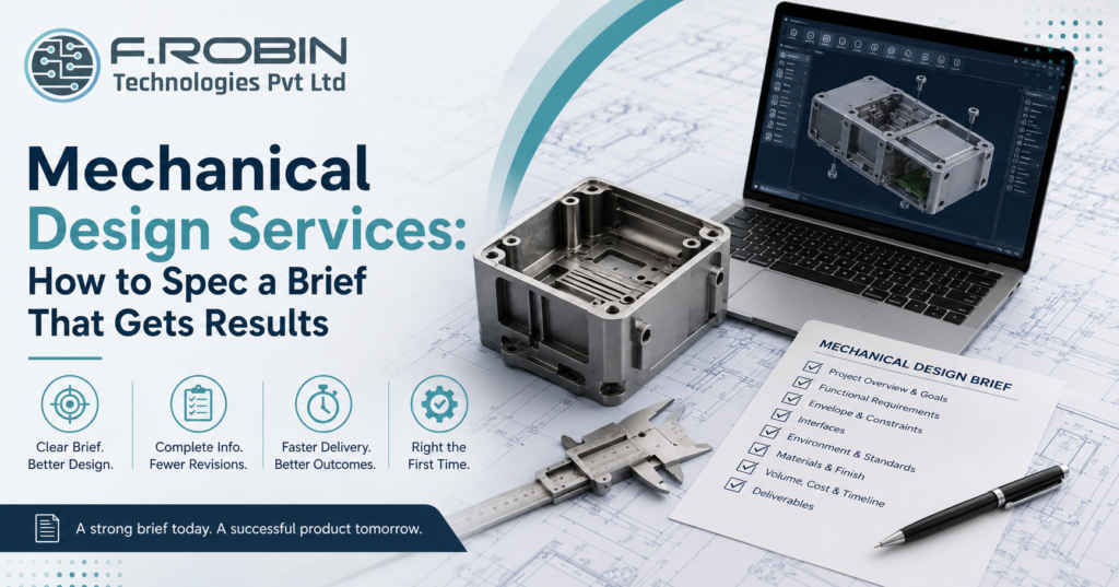
The quality of your mechanical design services engagement depends heavily on one thing you control: the brief you provide. Hand a design team a clear, complete brief, and you get accurate quotes, fewer revisions, and a product that fits the first time. Hand them a vague one, and you invite guesswork, delays, and costly rework. In short, a good brief is the single biggest lever you have over the outcome. This how-to guide shows exactly what to include in a mechanical design brief that gets results. We cover requirements, the envelope, interfaces, standards, and every other detail a mechanical design services team needs from you upfront — so your next project starts on solid ground and stays there. Why a Good Mechanical Design Brief Matters A brief is the foundation every design decision is built on. When it is clear, mechanical design services can move fast and confidently. When it is vague, they must either guess or stop and ask — and both cost time. The principle is simple: garbage in, garbage out. Missing requirements surface later as expensive redesigns, misfit parts, or failed compliance. A precise brief, by contrast, lets a mechanical design services team quote accurately, plan properly, and design right the first time. Think of the brief as an investment. The hour you spend making it complete saves days of back-and-forth and rework later. That is why the best projects always start with a strong brief, not a hopeful conversation. Before You Write the Brief A little preparation makes the brief far stronger. Before you start writing, gather the inputs that shape every decision: Assembling these first turns a blank page into a structured brief and prevents the mid-project surprises that come from missing context. What to Include in Your Brief A complete brief answers the questions a mechanical design services team will otherwise have to ask. Include each of the following. 1. Project Overview and Goals Start with the big picture: what the product is, who uses it, and what success looks like. This context helps a mechanical design services team make good decisions when details are unclear. 2. Functional Requirements List what the product must do — the functions, performance targets, and must-have features. Clear requirements are the backbone of any brief and the first thing a design team looks for. 3. The Envelope and Space Constraints Define the envelope: maximum dimensions, weight limits, and any space the design must fit within. If the product mounts somewhere specific, say so. Envelope constraints shape the entire concept. 4. Interfaces Detail every interface — how the design connects to the PCB, to other mechanical parts, and to the user. Strong PCB mechanical integration depends on sharing connector positions, mounting points, and board outlines here. 5. Environment and Standards Specify the operating environment (temperature, moisture, shock, vibration), the required IP rating, and any compliance standards the product must meet. These drive material, sealing, and testing choices. 6. Materials and Finish Note any material preferences, finish requirements, or brand/appearance needs. If you have no preference, say that too — it tells the team they have freedom to optimize. 7. Volume, Cost, and Timeline State expected production volume, target cost, and key dates. Volume changes the whole approach, so mechanical design services need it early to recommend the right process and materials. 8. Deliverables Expected Finally, list what you expect to receive: 3D CAD, drawings, prototypes, or production files. Clear deliverables prevent mismatched expectations at the end. Good vs Vague: An Example The difference between a weak and a strong brief is specificity. Compare two ways of stating the same requirement: The vague version forces the design team to guess — and guesses get corrected later at your expense. The specific version gives mechanical design services a clear, testable target they can design and verify against. Every requirement in your brief should be measurable like this: a number, a standard, or a pass/fail condition. Apply that precision line by line, and revision cycles fall away. A Mechanical Design Brief Checklist Use this checklist to confirm your brief is complete before you send it to a mechanical design services partner: If every box is ticked, your brief is ready. Any gaps are questions the design team would otherwise have to chase so fill them now. Common Brief Mistakes to Avoid Even experienced teams write weak briefs. Watch for these: Avoiding these keeps your mechanical design services project smooth and predictable. Most delays trace back to a gap in the brief — which is exactly why completeness pays off. How a Good Brief Speeds the Project A strong brief does more than prevent problems it accelerates the whole engagement. With complete information, mechanical design services can quote accurately, avoid clarifying delays, and design confidently from day one. The payoff shows up throughout the project: fewer revision cycles, better concept-to-production design, and a product that fits the first time. Because the team is not guessing, they spend their time engineering rather than chasing missing details. In practice, a good brief often shortens the timeline more than any other single factor. That makes writing it well one of the highest-return tasks you can do before engaging a mechanical design services team. It also builds trust: a supplier who receives a professional, complete brief treats the project — and the client — more seriously from the very first conversation. Key Takeaways Conclusion A great mechanical design brief is the highest-return work you can do before engaging mechanical design services. Cover the goals, requirements, envelope, interfaces, environment, standards, materials, volume, cost, and deliverables, and you give the design team everything they need to quote accurately and design right the first time. Skip these, and you invite guesswork and rework. The choice — and the outcome — is largely in your brief. Ready to Brief Your Project? Our Mechanical Engineering Services turn a clear project brief into concept-to-production results, ensuring seamless PCB mechanical integration throughout the development process. Collaborate with our experienced engineering team to accelerate
PCB Mechanical Integration: Avoiding Costly Fit Clashes
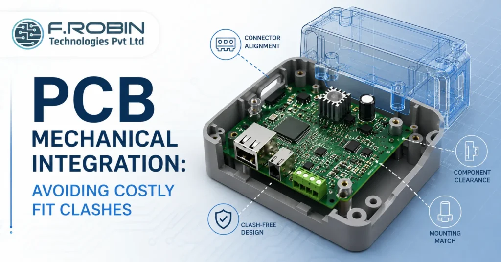
PCB mechanical integration is the practice of designing your board and its enclosure as one system, so they fit together perfectly the first time. When it goes well, connectors line up, components clear the lid, and assembly is effortless. When it goes wrong, you get fit clashes misaligned ports, components hitting the housing, mounting holes that miss and each one can trigger an expensive board or tooling respin. This guide explains how to get PCB mechanical integration right. We cover why fit clashes are so costly, what causes them, and the best practices that keep your board-to-enclosure design clash-free. Whether you build rugged industrial units or compact consumer devices, these techniques will save you time, money, and frustration. What Is PCB Mechanical Integration? PCB mechanical integration is the coordinated design of a printed circuit board and its mechanical enclosure so the two fit and function together. It ensures the board outline, components, connectors, and mounting points all align with the housing that surrounds them. In practice, this means the electrical and mechanical teams share information and a common 3D model throughout design. The board defines connector positions and component heights; the enclosure defines walls, cut-outs, and standoffs. PCB mechanical integration brings these two views together so nothing collides. Done well, it is invisible everything simply fits. Done poorly, it surfaces as clashes late in development, when fixes are most expensive. That is why treating board-to-enclosure design as one integrated task, not two separate ones, is the foundation of reliable hardware. Why Fit Clashes Are So Costly A single fit clash can be far more expensive than it first appears. Because mechanical and electrical issues often surface only after prototypes or tooling exist, fixing them means redoing expensive work. Poor PCB mechanical integration leads to costly outcomes: Each costs time and money that early integration would have prevented. The few hours spent coordinating board and enclosure up front save weeks of rework later — which is exactly why PCB mechanical integration deserves attention from day one. Common Causes of Fit Clashes Most fit problems trace back to a handful of recurring causes. Recognizing them early is half the battle. Almost all stem from designing the board and enclosure separately. When the two are integrated from the start, these clashes are caught on screen, not on the bench. PCB Mechanical Integration Best Practices Follow these best practices to keep board-to-enclosure design clash-free. Applied together, these practices turn PCB mechanical integration from a source of surprises into a predictable, repeatable process. They also tie directly into broader mechanical design services, where the enclosure and board evolve as one. The ECAD-MCAD Workflow The technical heart of PCB mechanical integration is exchanging data between electrical CAD (ECAD) and mechanical CAD (MCAD). The PCB tool holds the board and components; the MCAD tool — often SolidWorks — holds the enclosure. Keeping the two in sync is what prevents clashes. Teams typically share data using neutral formats: The goal is a single, shared source of truth. When the PCB moves a connector, the enclosure team sees it immediately; when the enclosure narrows a wall, the layout team adjusts. This continuous loop is what makes mechanical engineering and analysis of the assembly accurate and clash-free. Who Should Own the Integration? Fit clashes often slip through because no one clearly owns the board-and-enclosure handshake. The electrical team assumes the mechanical team is checking; the mechanical team assumes the opposite. Assigning one owner — or one shared review — closes that gap. On small teams, a single engineer comfortable in both ECAD and MCAD can own it. On larger projects, a brief integration review where both teams inspect the shared 3D assembly works well. Either way, make PCB mechanical integration a named responsibility with a checkpoint before release. When ownership is clear, clashes are caught early; when it is fuzzy, they reach the prototype bench — the most expensive place to find them. A Pre-Release Fit Checklist Before releasing the design, run through this quick checklist: Ticking every box before release is the simplest way to avoid a costly respin. If any item fails, fix it now — not after tooling. Common Mistakes to Avoid Even strong teams slip up on integration. Watch for these: Avoiding these keeps your PCB mechanical integration smooth and your project on schedule. Conclusion PCB mechanical integration is the difference between hardware that fits the first time and a project derailed by costly respins. By designing the board and enclosure as one system — sharing a 3D model, aligning connectors early, accounting for tolerance, and reviewing the full assembly before release — you eliminate the fit clashes that wreck schedules and budgets. Need Seamless PCB & Enclosure Integration? Avoid costly redesigns and mechanical fit issues. Our experts provide end-to-end Mechanical Engineering Services and PCB Layout Design Services to ensure your PCB, enclosure, and product architecture work together flawlessly from concept to production. Request a Design Consultation → Mechanical Engineering Services | PCB Layout Design Services Frequently Asked Questions 1. What is PCB mechanical integration? PCB mechanical integration is the coordinated design of a printed circuit board and its enclosure so they fit and function together, aligning the board outline, components, connectors, and mounting points with the housing. 2. Why is PCB mechanical integration important? It prevents costly fit clashes—misaligned connectors, components hitting the lid, or mismatched mounting holes—that would otherwise trigger board respins, tooling rework, and schedule delays. 3. What causes PCB-enclosure fit clashes? Common causes are connector misalignment, tall components, mismatched mounting holes, insufficient clearance, board outline errors, and tolerance stack-up—usually from designing the board and enclosure separately. 4. What is the ECAD-MCAD workflow? The ECAD-MCAD workflow exchanges data between electrical CAD (the PCB) and mechanical CAD (the enclosure, often in SolidWorks) using STEP and IDF/IDX formats, keeping both designs in sync. 5. How do I avoid connector alignment problems? Align connectors and ports with enclosure cut-outs early, share a common 3D model, and include tolerance margin so manufacturing variation does not cause
Electronic Enclosure Design: Concept to Production
Mechanical enclosure design is the process of creating the protective housing that holds and shields your electronics from first sketch to production-ready tooling. A good enclosure does far more than look tidy: it protects the board, manages heat, resists the environment, and shapes how users interact with the product. Get it wrong, and you risk failures, rework, and costly tooling changes. This guide walks through electronic enclosure design from concept to production, stage by stage. You will learn how requirements turn into 3D CAD, how to choose materials, how tolerance and ingress protection shape the design, and how a concept becomes a manufacturable housing. Whether you are building a rugged industrial unit or a sleek consumer device, the path is the same. What Is Mechanical Enclosure Design? Mechanical enclosure design is the engineering of a physical housing that protects and packages electronic hardware. It covers the enclosure’s shape, material, fit, fastening, sealing, and thermal behaviour everything that keeps the electronics safe and usable. The discipline blends form and function. On one hand, the enclosure must protect the board from dust, moisture, shock, and heat. On the other, it must be manufacturable, serviceable, and pleasant to use. Because it touches mechanical, thermal, and industrial design at once, enclosure design is a true cross-disciplinary task. It also works hand in hand with the electronics inside. The board outline, connector positions, and mounting points all influence the housing, so good electronic enclosure design starts with the PCB and the enclosure considered together never in isolation. Why Mechanical Enclosure Design Matters A well-designed enclosure protects your investment and your users. Skimp on it, and even a brilliant board can fail in the field. Strong mechanical enclosure design delivers several benefits: The cost of getting it wrong is high. Late enclosure changes after tooling are slow and expensive, and a poor seal or weak mount can cause field returns. Therefore, investing in mechanical enclosure design early protects both reliability and budget. The Mechanical Enclosure Design Process: Concept to Production Here is how concept-to-production design unfolds, stage by stage. Each step builds on the last. Step 1: Requirements and Specification Start by capturing requirements: size limits, environment, IP rating, thermal load, mounting, ports, certifications, and volume. A clear spec anchors every later decision and prevents costly surprises. Step 2: Concept Design Next, explore concepts. Sketches and rough 3D models test different forms, layouts, and split lines. This is the cheapest stage to experiment, so explore several directions before committing. Step 3: Detailed 3D CAD Now build the detailed model. Engineers create the enclosure in 3D CAD commonly SolidWorks defining walls, bosses, ribs, and features precisely. The PCB model is imported so the housing fits the board exactly. Step 4: Material Selection With the form set, choose the material. Material selection balances strength, cost, weight, thermal needs, and looks. We cover the main options below. Step 5: Tolerance and DFM Then refine for manufacturing. Tolerance analysis ensures parts fit reliably, while design for manufacturability (DFM) tunes features for the chosen process moulding, sheet metal, or machining. Step 6: Prototyping and Validation Build prototypes — often 3D printed or machined — and test fit, function, thermal, and ingress. Validation here catches issues while changes are still cheap, before tooling. Step 7: Production and Tooling Finally, commit to production. Tooling (such as injection moulds) is cut, first articles are inspected, and volume manufacturing begins. A clean handoff here turns your design into real, repeatable parts. Material Selection for Enclosures Material drives cost, durability, and process. The table compares common enclosure materials. Material Strengths Best For Injection-moulded Plastic Low unit cost at volume, excellent design freedom Consumer and high-volume products Sheet Metal Strong, good for shielding, low tooling cost Industrial and low-to-mid volume products Die-cast Aluminium Rugged, excellent thermal and EMI shielding Rugged, high-reliability units Aluminium Extrusion Cost-effective for long, simple shapes Rack units, amplifiers, and instruments There is no single best material — the right choice depends on volume, environment, and budget. For high-power products, thermal performance often drives the decision; for consumer goods, cost and finish lead. Ingress Protection (IP Ratings) Ingress protection defines how well an enclosure keeps out dust and water, expressed as an IP rating (for example, IP65). The first digit rates solids, the second rates liquids. Choosing the right rating early shapes seals, gaskets, and joints throughout the design. Common targets include: Over-specifying ingress protection adds cost and complexity, while under-specifying risks failure. Match the IP rating to the real operating environment, and design seals and gaskets to achieve it from the start — retrofitting sealing later is difficult and unreliable. Tolerance and Fit Tolerance is where good mechanical enclosure design succeeds or fails. Parts must fit together, align with the PCB, and accommodate manufacturing variation all at once. Loose tolerances cause rattles and gaps; overly tight tolerances raise cost without benefit. A tolerance stack-up analysis checks that the accumulated variation across mating parts still produces a reliable fit. It is especially important where the enclosure meets connectors, buttons, and the board, since misalignment here is highly visible to users. The goal is balance: specify tolerances tight enough to work, but loose enough to manufacture affordably. Coordinating closely with the PCB through solid PCB layout design services — keeps connector and mount positions aligned with the housing. Mechanical Enclosure Design and the PCB The single biggest predictor of enclosure success is how early it is coordinated with the board. Mechanical enclosure design and PCB layout should advance together, sharing the same 3D model so connectors, mounting holes, and tall components never clash with the housing. When the two teams work in sync, problems surface on screen instead of on the bench. Connector cut-outs line up, standoffs land on real pads, and tall capacitors clear the lid. When they work in isolation, the first prototype reveals expensive surprises. A shared 3D CAD workflow exporting the PCB into the enclosure model turns mechanical enclosure design from a guessing game into a precise, predictable process. This
PCB Mechanical Integration: Avoiding Costly Fit Clashes

PCB mechanical integration is the practice of designing your board and its enclosure as one system, so they fit together perfectly the first time. When it goes well, connectors line up, components clear the lid, and assembly is effortless. When it goes wrong, you get fit clashes misaligned ports, components hitting the housing, mounting holes that miss and each one can trigger an expensive board or tooling respin. This guide explains how to get PCB mechanical integration right. We cover why fit clashes are so costly, what causes them, and the best practices that keep your board-to-enclosure design clash-free. Whether you build rugged industrial units or compact consumer devices, these techniques will save you time, money, and frustration. What Is PCB Mechanical Integration? PCB mechanical integration is the coordinated design of a printed circuit board and its mechanical enclosure so the two fit and function together. It ensures the board outline, components, connectors, and mounting points all align with the housing that surrounds them. In practice, this means the electrical and mechanical teams share information and a common 3D model throughout design. The board defines connector positions and component heights; the enclosure defines walls, cut-outs, and standoffs. PCB mechanical integration brings these two views together so nothing collides. Done well, it is invisible — everything simply fits. Done poorly, it surfaces as clashes late in development, when fixes are most expensive. That is why treating board-to-enclosure design as one integrated task, not two separate ones, is the foundation of reliable hardware. Why Fit Clashes Are So Costly A single fit clash can be far more expensive than it first appears. Because mechanical and electrical issues often surface only after prototypes or tooling exist, fixing them means redoing expensive work. Poor PCB mechanical integration leads to costly outcomes: Each of these costs time and money that early integration would have prevented. In short, the few hours spent coordinating board and enclosure up front save weeks of rework later which is exactly why PCB mechanical integration deserves attention from day one. Common Causes of Fit Clashes Most fit problems trace back to a handful of recurring causes. Recognizing them early is half the battle. Almost all of these stem from designing the board and enclosure separately. When the two are integrated from the start, these clashes are caught on screen instead of on the bench. PCB Mechanical Integration Best Practices Follow these best practices to keep board-to-enclosure design clash-free. Applied together, these practices turn PCB mechanical integration from a source of surprises into a predictable, repeatable process. They also tie directly into broader mechanical design services, where the enclosure and board evolve as one. The ECAD-MCAD Workflow The technical heart of PCB mechanical integration is exchanging data between electrical CAD (ECAD) and mechanical CAD (MCAD). The PCB tool holds the board and components; the MCAD tool — often SolidWorks — holds the enclosure. Keeping them in sync is what prevents clashes. Teams typically share data using neutral formats: The goal is a single, shared source of truth. When the PCB moves a connector, the enclosure team sees it immediately; when the enclosure narrows a wall, the layout team adjusts. This continuous loop is what makes mechanical engineering and analysis of the assembly accurate and clash-free. A Pre-Release Fit Checklist Before releasing the design, run through this quick checklist: Ticking every box before release is the simplest way to avoid a costly respin. If any item fails, fix it now not after tooling. Common Mistakes to Avoid Even strong teams slip up on integration. Watch for these: Avoiding these keeps your PCB mechanical integration smooth and your project on schedule. Key Takeaways Conclusion PCB mechanical integration is the difference between hardware that fits the first time and a project derailed by costly respins. By designing the board and enclosure as one system — sharing a 3D model, aligning connectors early, accounting for tolerance, and reviewing the full assembly before release — you eliminate the fit clashes that wreck schedules and budgets. Building a Product Where the PCB and Enclosure Must Fit Perfectly? Our mechanical engineering services and PCB layout design services handle PCB mechanical integration from concept to production. Work with our engineering team to eliminate design clashes, reduce development risk, and accelerate time to market. Talk to Our Engineering Team Frequently Asked Questions 1. What is PCB mechanical integration? PCB mechanical integration is the coordinated design of a printed circuit board and its enclosure so they fit and function together, aligning the board outline, components, connectors, and mounting points with the housing. 2. Why is PCB mechanical integration important? It prevents costly fit clashes — misaligned connectors, components hitting the lid, or mismatched mounting holes — that would otherwise trigger board respins, tooling rework, and schedule delays. 3. What causes PCB-enclosure fit clashes? Common causes are connector misalignment, tall components, mismatched mounting holes, insufficient clearance, board outline errors, and tolerance stack-up — usually from designing board and enclosure separately. 4. What is the ECAD-MCAD workflow? The ECAD-MCAD workflow exchanges data between electrical CAD (the PCB) and mechanical CAD (the enclosure, often in SolidWorks) using STEP and IDF/IDX formats, keeping both designs in sync. 5. How do I avoid connector alignment problems? Align connectors and ports with enclosure cut-outs early, share a common 3D model, and include tolerance margin so manufacturing variation does not cause misalignment. “`
Electronics Enclosure Design in India: A Complete Guide to Housing Your PCB Safely
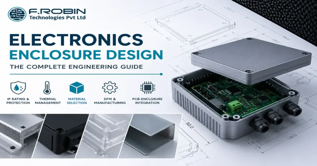
Electronics enclosure design in India is one of the most underestimated stages of hardware product development. Most engineering teams spend weeks optimising their PCB layout, then allocate a few days to the enclosure only to discover during production that the housing cracks under stress, traps heat around critical components, or fails its IP rating test because a cable gland was placed incorrectly. The enclosure is not packaging. It is an engineering system in its own right one that must manage heat, withstand mechanical stress, meet environmental protection ratings, comply with regulatory standards, accommodate manufacturing tolerances, and still look and feel like a finished product. Getting it wrong costs time, tooling money, and in some applications, product safety. This guide covers everything you need to know about electronics enclosure design material selection, IP ratings, thermal management, DFM rules, and how the enclosure and PCB design must work together from the earliest stages of development. 1. What Is Electronics Enclosure Design? Electronics enclosure design is the mechanical engineering discipline of designing the housing that protects and contains a printed circuit board and its associated components connectors, displays, switches, antennas, batteries, and wiring harnesses in a finished, deployable product. A well-designed enclosure serves several simultaneous functions. First, it provides mechanical protection shielding the PCB from physical impact, vibration, and handling damage. Additionally, it provides environmental protection sealing against dust, moisture, humidity, and chemical exposure. Furthermore, it manages thermal performance providing pathways for heat generated by components to dissipate safely. Finally, it ensures regulatory compliance meeting EMI/EMC shielding requirements, UL flammability ratings, and CE marking requirements for the target market. Why enclosure design must start alongside PCB layout The most expensive mistake in product development is treating enclosure design as an afterthought. Consequently, when the enclosure design begins after the PCB is finalised, the mechanical engineer is forced to design around a fixed board rather than co-designing the two together. This leads to: At F.Robin Technologies, PCB layout and mechanical enclosure design are integrated processes. Our engineering team co-designs the board and its housing simultaneously, which reduces respins and significantly shortens time to production. Learn more about our PCB design and layout services at frobintech.com/pcb-layout-design. 2. Enclosure Material Selection The choice of enclosure material is one of the most consequential decisions in the mechanical design process. Each material has specific trade-offs in mechanical strength, weight, thermal performance, cost, and manufacturability. Choosing the Right Material Aluminium (die-cast or machined) Aluminium is the preferred enclosure material for industrial, automotive, and outdoor electronics where thermal management, EMI shielding, and mechanical robustness are primary requirements. Die-cast aluminium is cost-effective at medium to high volumes, provides excellent heat dissipation (thermal conductivity 160–205 W/m·K), and offers natural EMI attenuation. Machined aluminium is used for low-volume, high-precision enclosures instrument housings, test equipment, and aerospace electronics where dimensional accuracy and surface finish are critical. However, machined aluminium is significantly more expensive per unit than die-cast at volume. ABS plastic (injection moulded) ABS (Acrylonitrile Butadiene Styrene) is the most common plastic enclosure material for consumer electronics, IoT devices, and indoor industrial products. It is lightweight, cost-effective at high volumes, easily coloured and textured, and straightforward to injection-mould with good dimensional consistency. ABS is not suitable for outdoor applications without UV-stabilised additives or protective coatings, and it provides minimal inherent EMI shielding (unlike metal). For applications requiring EMI shielding in a plastic enclosure, internal conductive coatings or gaskets are required. Polycarbonate (PC) Polycarbonate offers higher impact resistance than ABS, better optical clarity (relevant where display windows or light pipes are required), and superior heat resistance. It is commonly used in enclosures for outdoor lighting, medical devices, and safety equipment. PC is more expensive than ABS and can be more challenging to mould without warping in thick sections. PC/ABS blends PC/ABS blends combine the impact resistance of polycarbonate with the processability and lower cost of ABS. They are widely used in handheld devices, ruggedised consumer electronics, and industrial handhelds where both aesthetics and durability matter. Sheet metal (steel or aluminium) Sheet metal enclosures bent and welded from steel or aluminium sheet are cost-effective for low-to-medium volumes and allow rapid design iteration without expensive tooling. Standard sheet metal enclosures are widely available off-the-shelf for DIN rail mounting and 19-inch rack mounting. Custom sheet metal enclosures require only laser cutting and bending fixtures, not injection moulding tools, making them faster and cheaper to prototype. Material comparison table Material Thermal Conductivity EMI Shielding IP Achievable Relative Cost (High Volume) Best For Die-cast Aluminium Excellent Excellent IP67+ Medium Industrial, automotive, outdoor applications Machined Aluminium Excellent Excellent IP67+ High Low-volume, precision instruments ABS Plastic Poor Poor (unless coated) IP65 with gasket Low Consumer electronics, indoor IoT devices Polycarbonate Poor Poor (unless coated) IP67 with gasket Low–Medium Outdoor equipment, medical devices, lighting Sheet Metal (Steel) Good Good IP54 typical Low–Medium Industrial panels, 19-inch rack enclosures 3. IP Ratings Explained Choosing the Right Protection Level IP (Ingress Protection) rating is defined by IEC 60529 and specifies the degree of protection an enclosure provides against solid particles and liquids. Understanding IP ratings is essential before finalising the enclosure design, because the target IP rating directly drives gasket selection, cable gland specification, parting line placement, and surface finish requirements. How IP ratings work An IP rating consists of two digits. The first digit (0–6) specifies protection against solid particles from no protection (0) to complete dust-tight protection (6). The second digit (0–9K) specifies protection against liquids from no protection (0) to high-pressure, high-temperature water jets (9K). Common IP ratings and their applications IP54 — Dust protected, splash proof Protection against limited dust ingress and water splashing from any direction. Suitable for indoor industrial environments motor drives, PLC enclosures, factory automation. The most commonly achieved rating for sheet metal and plastic enclosures without specialist gaskets. IP65 — Dust tight, low-pressure water jet Complete dust protection and resistance to low-pressure water jets from any direction. Required for outdoor equipment not directly exposed to rain outdoor lighting, roadside infrastructure, solar inverters. Requires a continuous perimeter gasket
Finite Element Analysis Services: The Complete Guide for Product Engineers [2026]

What Is Finite Element Analysis (FEA)? Finite Element Analysis (FEA) is a computational simulation technique that predicts how a product or structure will behave under real-world conditions before a single physical prototype is built. The underlying method divides a complex component into thousands of small, simple shapes called finite elements. Each element is mathematically analyzed under applied forces, temperatures, pressures, or vibrations. The results are then assembled across the entire model to produce detailed maps of stress, displacement, heat distribution, or fatigue life. In plain terms: FEA tells you whether your design will hold up or fail without the cost and delay of building and breaking actual parts. It is one of the most powerful tools in the modern engineering toolkit. From automotive crumple zones to satellite brackets, from pressure vessels in oil refineries to heat sinks in PCB enclosures, FEA underpins the safety and reliability of almost every engineered product in service today. How Does FEA Work? Step-by-Step Process Understanding the FEA workflow helps you communicate effectively with your simulation team and set realistic expectations for timelines and deliverables. Step 1 — CAD Model Preparation The process begins with a 3D CAD model of the component or assembly. Engineers simplify the geometry by removing non-structural features (small holes, fillets, logos) that add computation time without meaningfully affecting results. This step is called defeaturing or geometry clean-up. Step 2 — Material Definition Every element in the model needs material properties: Young’s modulus, Poisson’s ratio, yield strength, thermal conductivity, density, and more. Getting this right is critical an FEA model is only as accurate as the material data feeding it. Step 3 — Meshing The geometry is divided into finite elements. Mesh quality element size, shape, and density directly controls result accuracy. Critical regions (stress concentrations, welds, contact zones) need finer meshes. Poor meshing is one of the most common sources of error in FEA. Step 4 — Boundary Conditions and Loads Engineers define how the component is constrained (fixtures, bolted joints, welded connections) and what loads are applied (forces, pressures, temperatures, moments). Incorrect boundary conditions are the biggest cause of misleading FEA results. Step 5 — Solving The FEA solver (ANSYS, Abaqus, NASTRAN, etc.) assembles and solves a system of equations often millions of them for large models. This step runs computationally on high-performance workstations or cloud clusters. Step 6 — Post-Processing and Interpretation The solver outputs are visualized as color-coded contour plots (von Mises stress, temperature, displacement). Engineers interpret these results in the context of safety factors, material limits, and design codes (ASME, ISO, EN). Step 7 — Design Recommendations A professional FEA service doesn’t just hand you a stress map. The final deliverable includes an engineering report identifying failure risks, suggested design changes, and quantified safety margins. Types of Finite Element Analysis Not all FEA is the same. The type of simulation required depends on what could go wrong with your product. Here are the six most commonly used FEA types in mechanical engineering services. 1. Static Structural Analysis (Linear & Nonlinear) The most widely used type. Static analysis applies loads that don’t change over time and checks for stress, strain, and deformation. Linear static analysis assumes the material behaves elastically and deformations are small — suitable for most standard components under normal operating loads. Nonlinear static analysis is required when dealing with large deformations, material plasticity (permanent yielding), or complex contact between parts. It is computationally heavier but necessary for realistic results in demanding conditions such as press-fit assemblies, rubber components, or highly loaded structures. Typical use cases: structural brackets, frames, pressure vessels, machine parts, enclosure housings. 2. Thermal Analysis Thermal FEA simulates heat transfer through conduction, convection, and radiation. It can be run as a standalone analysis or coupled with structural analysis (thermo-mechanical analysis) to evaluate thermal stresses. Typical use cases: PCB enclosure thermal management, heat exchangers, turbine components, engine blocks. 3. Dynamic and Vibration Analysis Dynamic FEA evaluates how a structure responds to time-varying loads. The three primary subtypes are: Typical use cases: rotating machinery, aerospace structures, automotive NVH (noise, vibration, harshness), industrial equipment. 4. Fatigue Analysis Fatigue is responsible for the majority of mechanical failures in service. Fatigue FEA predicts how many load cycles a component can withstand before a crack initiates and propagates to fracture. Two main methodologies are used: stress-life (S-N) for high-cycle fatigue in components that experience millions of load cycles, and strain-life (ε-N) for low-cycle fatigue where plastic deformation occurs each cycle. Fatigue analysis is standard practice in automotive, aerospace, and rotating equipment design. Typical use cases: suspension components, aircraft structures, pressure vessels under cyclic loading, pump impellers. 5. Buckling Analysis Buckling analysis identifies the critical load at which a slender or thin-walled structure suddenly collapses under compressive forces — even before yielding occurs. The classic example is a column that bows and snaps under compressive load well below its material yield strength. Typical use cases: aerospace panels, structural columns, thin-walled pressure vessels, offshore risers. 6. Computational Fluid Dynamics (CFD) — Coupled Analysis While CFD is technically a separate discipline, it is frequently coupled with structural FEA in a workflow called Fluid-Structure Interaction (FSI). Pressure loads computed by CFD (airflow over a wing, fluid inside a pipe) are mapped onto an FEA model for structural validation. Typical use cases: offshore pipelines, HVAC ductwork, turbine blades, heat exchanger tube bundles. Industries That Use FEA Services FEA services are used across virtually every engineering-intensive industry. Here are the sectors where simulation-driven design delivers the greatest return. Aerospace and Defense Every primary flight structure must be analytically justified before it flies. FEA is used to validate wing spars, fuselage frames, landing gear, and satellite structures against stringent certification requirements (FAA, EASA, MIL-STD). Solver dominance: NASTRAN with Femap/Patran pre/post-processing. Automotive Three FEA workstreams define automotive engineering: crashworthiness (explicit dynamics, LS-DYNA), NVH (noise, vibration, harshness), and fatigue durability. A single body-in-white model may be reused across all three with different load cases and solver settings. Oil, Gas, and Process Industries ASME Section VIII pressure
