
Impedance control is one of the most important — and most misunderstood — topics in PCB design. As signals get faster, the copper traces carrying them start to behave like transmission lines, and their impedance directly affects whether data arrives cleanly or arrives corrupted. Get impedance control right in your PCB design, and high-speed interfaces just work. Get it wrong, and you face reflections, noise, and failures that are painful to debug.
This guide explains impedance control in plain terms: what it is, why it matters, what affects it, and how to specify it correctly on your fabrication drawing. Whether you are routing DDR memory, USB, PCIe, or Ethernet, controlled impedance is the foundation that keeps those signals reliable.
What Is Impedance Control in PCB Design?
Impedance control in PCB design is the practice of designing traces so they present a specific, consistent characteristic impedance to the signals they carry — for example, 50 ohms. A controlled-impedance trace behaves like a transmission line, delivering signals without distortion.
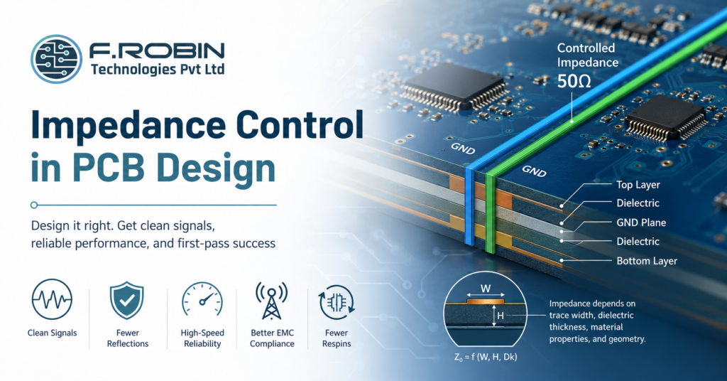
Characteristic impedance depends on the trace’s geometry and the materials around it. By controlling trace width, spacing, copper thickness, and the dielectric between layers, a designer sets the impedance to a target value. This is why controlled impedance is a stack-up decision as much as a routing one.
In everyday PCB design, you do not control impedance on every trace — only on the high-speed nets that need it. Identifying those nets early, and designing them as controlled-impedance lines, is the heart of impedance control.
Why Impedance Control Matters
Impedance control matters because mismatched impedance causes signal reflections. When a fast signal meets a change in impedance, part of its energy bounces back, distorting the waveform. At high speeds, those reflections corrupt data and cause intermittent, hard-to-find failures.
Good impedance control in your PCB design delivers real benefits:
- Clean signals that meet timing and voltage margins.
- Fewer reflections, ringing, and overshoot.
- Reliable high-speed links like DDR, USB, PCIe, and Ethernet.
- Easier EMC compliance, since controlled signals radiate less.
- Fewer respins, because problems are designed out, not debugged out.
The faster your edges, the more impedance matters. For modern interfaces, controlled impedance is not optional it is the difference between a board that works and one that fails unpredictably.
What Affects PCB Impedance?
Several physical factors set a trace’s impedance. Understanding them is essential to good PCB design.
- Trace width. Wider traces lower impedance; narrower traces raise it.
- Dielectric thickness. The distance to the reference plane strongly affects impedance.
- Dielectric constant (Dk). The material’s electrical property shifts the result.
- Copper thickness. Heavier copper slightly changes impedance.
- Trace geometry. Microstrip (outer layer) and stripline (inner layer) behave differently.
Because these factors interact, impedance is calculated from the whole stack-up, not from trace width alone. This is also why the multilayer PCB stack-up you choose directly determines which impedances you can achieve.
Single-Ended vs Differential Impedance
There are two impedance types you will specify in PCB design. Single-ended impedance describes one trace referenced to a ground plane — common for clocks and simple signals. Differential impedance describes a pair of traces carrying equal and opposite signals, used for high-speed interfaces like USB and PCIe.
Differential pairs need both the right individual impedance and the right coupling between the two traces. Therefore, spacing matters as much as width. Getting the pair geometry right keeps the differential impedance on target and the signals balanced.
Common Impedance Values
Most high-speed interfaces target standard impedance values. The table lists common ones.
| Signal Type | Typical Impedance |
|---|---|
| Single-ended (general) | 50 Ω |
| USB differential | 90 Ω |
| PCIe / Ethernet differential | 100 Ω |
| DDR (varies by standard) | 40–50 Ω (single-ended) |
How to Specify Controlled Impedance Correctly
Specifying impedance correctly is where many PCB design projects slip. To get it right, your fabrication drawing should clearly state:
- The target impedance for each controlled net or layer (e.g., 50 Ω single-ended).
- The tolerance, commonly ±10%.
- Which layers carry controlled-impedance traces.
- The reference planes each net uses.
- A request for impedance coupons, so the fab can test and verify.
Crucially, let your manufacturer adjust trace widths to hit the target on their actual stack-up. Fabs build to slightly different materials, so a good practice is to specify the impedance and let them tune the geometry. A clean handoff to PCB manufacturing ensures the impedance you designed is the impedance you receive.
Impedance and Simulation
Simulation confirms that your impedance choices will work before you build. Pre-layout simulation explores stack-up and topology options, while post-layout simulation verifies the routed design against its targets.
For demanding boards, pairing impedance control with high-speed PCB analysis catches reflections, crosstalk, and timing issues early. This pre/post layout simulation workflow turns impedance from a hopeful guess into a verified result — and it is far cheaper than discovering a problem after fabrication. For complex high-speed designs, dedicated signal integrity analysis is the gold standard.
Where Impedance Control Fits in the PCB Design Flow
Impedance control is not a final step you bolt on at the end — it threads through the whole PCB design flow. It starts at the requirements stage of PCB design, when you identify which interfaces are high-speed and what impedance each one demands. It continues into stack-up design, where dielectric thicknesses and reference-plane positions set what impedance is even achievable.
During layout, you route the controlled nets first, holding trace width and spacing steady so the impedance stays on target. Finally, you verify with simulation and impedance coupons. Treating impedance as a thread running through your PCB design — rather than an afterthought — is what separates boards that work the first time from those that need a costly respin.
Best Practices for Impedance Control
Apply these practices in your PCB design:
- Identify controlled nets early, before finalizing the stack-up.
- Pair every high-speed signal with a solid reference plane for a clean return path.
- Avoid plane splits under controlled-impedance traces.
- Keep differential pairs tightly and consistently coupled.
- Specify impedance, not just width, and let the fab tune geometry.
- Request impedance coupons to verify the result.
Following these keeps your controlled-impedance design accurate and manufacturable. They also tie directly into the broader printed circuit board design workflow.
Common Mistakes to Avoid
Watch for these frequent impedance errors:
- Controlling impedance by width alone, ignoring the dielectric and stack-up.
- Routing high-speed traces over plane splits, breaking the return path.
- Forgetting to specify impedance on the fabrication drawing.
- Mismatched differential pair spacing, throwing off coupling.
- Skipping impedance coupons, so the result is never verified.
- Leaving impedance to chance instead of simulating it.
Avoiding these keeps your PCB design reliable and your high-speed signals clean.
Conclusion
Impedance control is a cornerstone of reliable high-speed PCB design. By designing controlled-impedance traces, pairing them with solid reference planes, and specifying the target impedance and tolerance on your fabrication drawing, you keep fast signals clean and avoid costly reflections and respins. Remember that impedance comes from the whole stack-up — so plan it early and verify it with simulation and coupons.
Frequently Asked Questions
1. What is impedance control in PCB design?
Impedance control in PCB design is the process of designing PCB traces to maintain a specific, consistent characteristic impedance—such as 50 Ω—so high-speed signals travel with minimal distortion, reflections, and signal loss.
2. Why is controlled impedance important?
Controlled impedance prevents signal reflections that can corrupt high-speed data. It improves signal integrity, supports reliable interface performance, simplifies EMC compliance, and reduces costly PCB redesigns.
3. What affects impedance on a PCB?
PCB impedance is influenced by trace width, dielectric thickness, dielectric constant (Dk), copper thickness, and trace geometry, such as microstrip or stripline. Proper stack-up design is essential for accurate impedance control.
4. What is the difference between single-ended and differential impedance?
Single-ended impedance refers to a single trace referenced to a ground plane, while differential impedance is measured across a pair of traces carrying equal and opposite signals. Differential impedance depends on both trace width and spacing.
5. What are common PCB impedance values?
Typical controlled impedance targets include 50 Ω for single-ended signals, 90 Ω for USB differential pairs, and 100 Ω for PCIe and Ethernet differential pairs. Always follow your interface specification and PCB manufacturer’s stack-up recommendations.
