
Custom PCB Design Services: When Off-the-Shelf Won’t Cut It
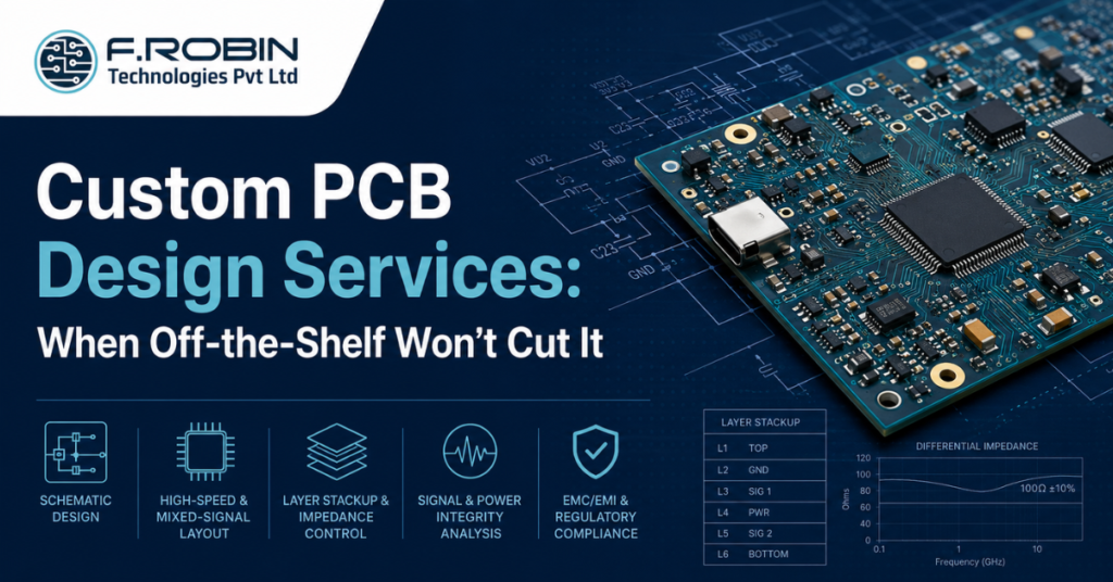
There is a moment in every hardware product cycle when a development module stops being a solution and starts being a constraint. The form factor is wrong. Unit costs are eroding margin. The RF noise is killing your analog front end. Your certification lab just handed back a failure report. That moment is when custom PCB design services become the only logical path forward. This guide helps hardware engineers, product managers, and procurement leads decide when to move from commercial modules to a purpose-built electronic PCB design — and what a professional engagement actually involves. What Are Custom PCB Design Services? Custom PCB design services are the end-to-end engineering process of designing a printed circuit board from the ground up — tailored to your product’s exact electrical, mechanical, thermal, and regulatory requirements. A professional PCB design company typically delivers: Custom electronic PCB design is not always necessary. But when it is, the gains in performance, size, cost, and certification compliance are difficult to achieve any other way. Off-the-Shelf vs. Custom PCB Design: Direct Comparison Factor Off-the-Shelf Module Custom PCB Design Time to Prototype Days to weeks 4–12 weeks NRE Cost None Moderate to high Unit Cost at Volume High (module premium) Low (optimized BOM) Form Factor Control Fixed Full control Regulatory Certification Often pre-certified Requires own testing IP Protection Low High proprietary design Mixed-Signal Performance Compromised Fully optimized Long-Term Supply Risk Module discontinuation Component-level sourcing Bottom line: For prototypes or low-volume internal tools, commercial modules are often the right call. For production-bound, certification-required, or cost-sensitive products, custom PCB design services pay for themselves. 7 Signs You Need Custom PCB Design Services 1. Your Form Factor Is Fixed and Modules Don’t Fit Medical wearables, aerospace enclosures, industrial handheld instruments — these have non-negotiable physical envelopes. When no commercial module fits, a custom PCB designed to exact mechanical constraints is the only option. 2. You’re Paying Module Premium at Production Volume Modules are priced for flexibility and small quantities. At 5,000+ units annually, the per-unit cost premium typically exceeds the original NRE investment within 12–18 months. 3. Your Design Has High-Speed Digital Signals Above 100 MHz — or with interfaces like DDR4, PCIe, USB 3.x, or MIPI — impedance-controlled routing and proper layer stackup are non-negotiable. These requirements demand high-speed digital and mixed-signal PCB layout expertise that commercial modules cannot substitute. 4. You’re Mixing Analog and Digital Domains Mixed-signal PCB design is among the most demanding disciplines in electronic PCB design. Poor ground plane management or insufficient isolation between analog and digital sections can destroy ADC performance or cause EMI failures. 5. Your Product Must Pass Regulatory Certification FCC Part 15, CE marking, IEC 60601 — certification evaluates the entire assembly. A PCB designed with EMC compliance in mind (shielding zones, controlled impedance, ferrite placement) has a significantly higher first-pass compliance rate. 6. You Have a Supply Chain or IP Concern Module vendors can discontinue products or become sole-source dependencies. Custom PCB design distributes sourcing risk across multiple suppliers and protects your architecture as proprietary IP. 7. Your Product Competes on Performance If your market position depends on a lower noise floor, faster processing, tighter latency, or higher precision, every compromised trace and shared power rail is a competitive liability. Custom PCB design services exist to remove these compromises. What Professional PCB Design Services Include Engaging a qualified PCB design company delivers more than a routed layout file. A full engagement covers: Schematic Capture and Review The design process starts with a verified schematic. The PCB design team reviews all reference designs, application notes, and datasheet recommendations. Errors caught here cost a fraction of what they cost after fabrication. Layer Stackup and Impedance Planning For high-speed or RF designs, the stackup is engineered before a single trace is routed. Layer count, dielectric material, copper weights, and layer assignments determine whether controlled impedance targets (50Ω single-ended, 100Ω differential) are achievable. Component Placement and Routing Experienced PCB designers apply thermal management, signal integrity, and DFM principles simultaneously during placement and routing. High-speed nets require length matching, guard routing, and verified return path continuity. DFM Review and Gerber Output A complete deliverable package includes fabrication-ready Gerber files, drill files, a BOM with approved alternates, assembly drawings, and a fabrication specification. High-Speed Digital and Mixed-Signal PCB Layout: Why It Matters High-speed digital and mixed-signal PCB layout combines signal integrity engineering, EMC design, and analog circuit principles — and is where most first-time custom PCB projects encounter problems. Key principles every PCB design company should apply: A poorly routed DDR5 interface can cause data corruption at speed. A shared ground between a switching regulator and a low-noise amplifier can inject hundreds of millivolts of noise into your signal chain. These are not edge cases — they’re common failure modes in designs that skip specialist mixed-signal PCB layout review. Key Takeaways Ready to Move from Module to Custom? If a commercial module is limiting your product’s performance, inflating costs, or blocking certification, it’s time to work with a PCB design team that understands the full engineering picture. Request a Design Consultation →
