
Multilayer PCB Design: How Many Layers Do You Really Need?
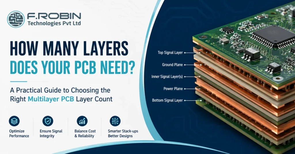
Choosing the right multilayer PCB layer count is one of the most consequential decisions in any hardware project. Pick too few layers and you fight routing congestion, noise, and signal problems. Pick too many and you inflate cost for no real benefit. So how many layers do you really need? The short answer: most products land on 4 layers, but the right number depends on signal speed, routing density, power complexity, and budget. In this decision guide, we walk through a practical framework for sizing a multilayer PCB, share common stack-up configurations, and show where the cost-versus-performance line really sits. By the end, you will be able to justify your layer count with confidence. What Is a Multilayer PCB? A multilayer PCB is a circuit board with three or more conductive copper layers separated by insulating material and bonded into a single board. Unlike a single- or double-sided board, a multilayer circuit board stacks signal layers, power planes, and ground planes vertically to pack more connections into less space. These extra layers do two important jobs. First, they give you more room to route dense designs. Second, dedicated power/ground planes deliver cleaner power and shorter return paths, which improves signal quality and reduces noise. Consequently, almost every modern product — from a smartphone to an industrial controller — relies on multilayer PCB design. The term layer stack (or stack-up) describes exactly how those layers are arranged. Getting the layer stack right is the heart of good multilayer PCB design, because it sets impedance, return paths, and manufacturability all at once. Why Layer Count Matters Layer count is not just a routing detail — it shapes performance, cost, and reliability together. Because each pair of layers adds material and process steps, every extra layer increases the price of your multilayer circuit board. Therefore, you want the lowest layer count that still meets your electrical goals. More layers deliver clear advantages: However, the benefits taper off. Adding layers a design does not need wastes money and lengthens lead times. As a result, smart multilayer PCB design is a balancing act enough layers to perform well, but no more than necessary. How Many Layers Do You Really Need? Use this framework to size your multilayer PCB. Work through the factors first, then match them to the layer-count guide below. Step 1: Assess the Key Factors Five factors drive layer count: Step 2: Match Factors to a Layer Count Layers Best For What You Get 2 Simple, low-speed, cost-sensitive boards Signal routing on both sides; no dedicated power or ground planes 4 Most products Two signal layers plus dedicated power and ground planes 6 Moderately complex designs with some high-speed nets Additional signal layers with multiple reference planes 8 High-speed digital designs and dense routing Strong impedance control, improved signal integrity, and isolation 10–16+ Multi-layer multi-processor board design, HDI, telecom systems Maximum routing density, multiple planes, shielding, and performance Step 3: Add a Margin If your design sits on the edge between two counts, choose the higher one. A single respin to add layers costs far more than the modest material premium of starting with enough. This is especially true for high-speed work, where you can also pair the layout with signal integrity analysis to confirm the stack-up performs as intended. Common Multilayer PCB Stack-Up Configurations The way you arrange signal layers and power/ground planes matters as much as the layer count. Here are proven layer stack patterns. 4-Layer Stack-Up A classic 4-layer multi layer pcb board uses: Signal – Ground – Power – Signal. The ground plane sits directly under the top signal layer, giving high-speed traces a clean return path. This arrangement suits the majority of products. 6-Layer Stack-Up A common 6-layer layer stack is: Signal – Ground – Signal – Signal – Power – Signal. It adds two more routing layers while keeping references close to critical signals. Use it when a 4-layer board runs out of room or needs better isolation. 8-Layer and Beyond High-speed and multi-layer multi-processor board design often needs 8 or more layers to provide multiple ground and power planes between signal layers. This sandwiching maximizes shielding and impedance control. As density climbs, HDI techniques and blind/buried vias frequently join the stack. PCB Design Tip Rule of thumb: Every signal layer should sit adjacent to a reference plane. If it does not, revisit your layer stack. Keeping signal layers next to ground or power planes improves return-current paths, impedance control, signal integrity, and EMI performance. Cost vs Performance: The Multilayer PCB Trade-off Each step up the layer ladder buys performance but raises cost and lead time. The table below summarizes the trade-off so you can decide where your project belongs. Layer Count Relative Cost Performance Ceiling Typical Lead Time 2 Lowest Low-speed designs only Shortest 4 Moderate Suitable for most designs Standard 6 Higher High-speed capable Slightly longer 8+ Highest Maximum routing density and signal integrity Longest In practice, jumping from 2 to 4 layers gives the biggest performance return for the smallest cost increase. Beyond 6 layers, add layers only when density or signal requirements truly demand them. When you are ready to build, a clean PCB manufacturing handoff keeps those layer costs predictable. Best Practices for Multilayer PCB Design Apply these practices to get the most from every layer: Common Mistakes to Avoid Even experienced teams stumble on layer-count decisions. Watch for these: Avoiding these mistakes keeps your multilayer circuit board reliable, manufacturable, and on budget. Key Takeaways Conclusion Sizing a multilayer PCB comes down to a clear decision: assess signal speed, routing density, power complexity, EMI, and cost, then choose the lowest layer count that meets your goals — and round up when you are on the edge. Most products are well served by 4 layers, while high-speed and multi-layer multi-processor board designs justify 6, 8, or more. Above all, keep every signal layer next to a reference plane and the layer stack symmetrical. Need Help Planning Your PCB Layer Stack? Need help
Printed Circuit Board Design: A Step-by-Step Workflow
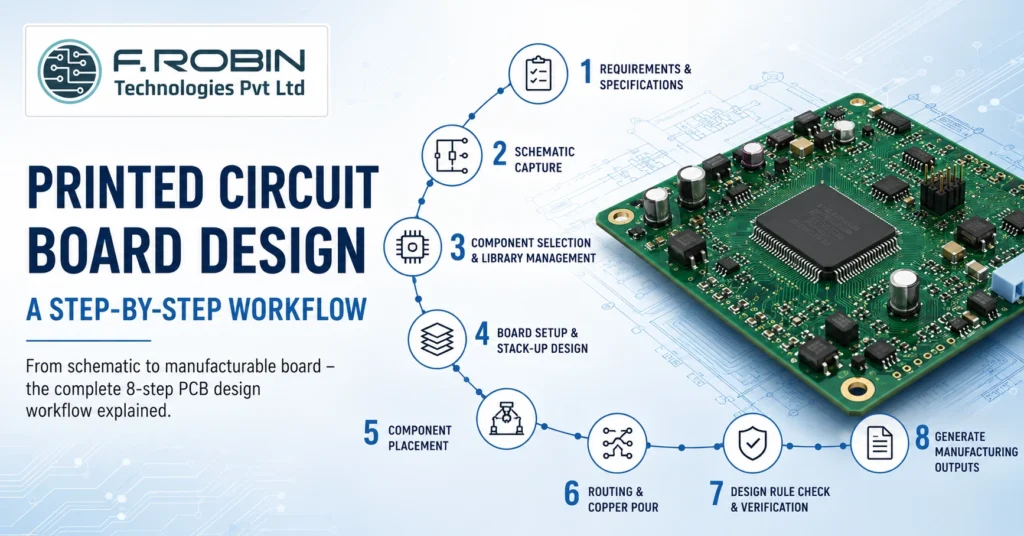
Printed circuit board design is the structured process of turning a circuit idea into a manufacturable board that powers almost every electronic product you use. Whether you are building a simple sensor module or a complex multi-layer system, the workflow follows the same logical path. Moreover, getting that path right the first time saves weeks of rework and thousands in respin costs. In this guide, we break down the complete printed circuit board design workflow into eight clear stages. You will learn what happens at each step, why it matters, and how to avoid the mistakes that trip up even experienced engineers. By the end, you will understand exactly how a schematic becomes a finished board ready for the factory. What Is Printed Circuit Board Design? Printed circuit board design is the process of creating the electrical and physical layout of a PCB so it can be reliably manufactured and assembled. In short, it converts a schematic — a diagram of how components connect — into a precise set of copper traces, layers, and footprints on a board. The process spans two linked activities. First, schematic design defines the logical connections between components. Second, board layout design places those components and routes the copper that joints them. Together, these stages form the foundation of every working electronic product. A complete PCB design also includes the manufacturing data the factory needs, such as Gerber files, drill files, and a bill of materials. Consequently, good design is about far more than drawing traces — it is about producing a board that works, lasts, and can actually be built at scale. Why the Printed Circuit Board Design Workflow Matters Following a disciplined workflow is the single biggest factor in first-pass success. Because each stage feeds the next, a small error early on multiplies downstream. For example, a wrong footprint chosen during component selection can force a complete respin after fabrication. A structured PCB design process delivers clear benefits: In high-speed and mixed-signal products, the stakes rise further. Therefore, many teams pair their layout work with signal integrity analysis to verify performance before the board is ever built. The 8-Step Printed Circuit Board Design Workflow Here is the end-to-end printed circuit board design workflow, stage by stage. Each step builds on the last, so resist the urge to skip ahead. Step 1: Define Requirements and Specifications Start with a clear specification. Capture the board’s function, operating voltages, signal speeds, environmental conditions, size limits, and target cost. Additionally, note any standards the board must meet, such as IPC Class 2 or Class 3. A solid spec becomes the reference you check every later decision against. Step 2: Schematic Capture Next, draw the schematic. During schematic capture, you place component symbols and wire their connections to define the netlist — the master list of every electrical connection. Use clear net names, add design notes, and run an electrical rule check (ERC) to catch missing connections or conflicting outputs early. Step 3: Component Selection and Library Management Now choose real parts for every symbol. Verify availability, footprint accuracy, and electrical ratings. Crucially, use trusted library data — a wrong land pattern is one of the most common causes of unassemblable boards. Strong library management keeps footprints, symbols, and 3D models consistent across projects. Step 4: Board Setup and Stack-Up Design Define the physical board: outline, layer count, and stack-up. The stack-up sets how signal, power, and ground layers are arranged, along with dielectric thicknesses. For high-speed nets, this is where you plan controlled impedance. As a rule, every signal layer should have an adjacent reference plane for a clean return path. Layer Count Typical Use 2 Layers Simple, low-speed, cost-sensitive boards 4 Layers Most products; dedicated power and ground planes 6–8 Layers High-speed digital, dense routing, controlled impedance 10+ Layers Complex multi-processor and HDI designs Step 5: Component Placement With the board set up, position your parts. Good placement drives everything that follows. Group related circuits, keep high-speed paths short, separate analog from digital, and place connectors and mounting holes per the mechanical drawing. Smart placement makes routing easier and improves thermal and signal performance at the same time. Step 6: Routing and Copper Pour Now connect the dots. Routing lays the copper traces that carry each signal, while a copper pour fills open areas — usually with ground — to improve return paths, shielding, and heat spreading. Match trace widths to current, control impedance on critical nets, and avoid sharp acute angles. Route power and high-speed signals first, then fill in the rest. Step 7: Design Rule Check and Verification Before release, run a design rule check (DRC). The DRC flags violations such as traces too close together, undersized clearances, or unconnected nets. Fix every error, then verify against your original spec. For demanding boards, add pre/post-layout simulation to confirm signal and power integrity. Step 8: Generate Manufacturing Outputs Finally, export the data the factory needs: Gerber (RS-274X) or ODB++ files, an NC drill file, a bill of materials, and assembly drawings. Review these outputs carefully, because they are what actually gets built. A clean handoff here connects your design directly to PCB manufacturing and assembly. PCB Design Tools Compared Your toolset shapes how efficiently you move through the PCB design workflow. The table below compares three widely used options. Tool Best For Notes Altium Designer Professional, high-speed, and complex multi-layer boards Unified environment with strong routing and library management OrCAD (Cadence) Enterprise teams needing advanced simulation Tight integration with Cadence analysis tools KiCad Startups, makers, and budget-conscious teams Free and open-source with a fast-growing feature set There is no single “best” tool — the right choice depends on board complexity, budget, and team workflow. Many engineers learn on KiCad and graduate to OrCAD or Altium Designer for high-speed production work. Best Practices for Printed Circuit Board Design Apply these proven practices to raise quality on every project: For products with tight enclosures, coordinate early with mechanical integration so the board fits and cools correctly.
How to Choose a PCB Design Company (12-Point Checklist)

Choosing the right PCB design company can make or break your hardware project. The right partner ships clean, manufacturable boards on time; the wrong one drains your budget with respins, missed deadlines, and IP worries. So before you sign anything, you need a way to separate a capable PCB design company from a risky one. This 12-point checklist gives you exactly that. We cover technical capability, trust and IP protection, process and communication, and commercial and local fit. Whether you are searching for a “pcb design company near me,” evaluating a PCB design firm in Chennai, or comparing offshore PCB design services, these 12 questions will help you commit with confidence. Why Choosing the Right PCB Design Company Matters Your PCB design company shapes the cost, reliability, and time-to-market of your entire product. Because layout errors surface only after fabrication, a weak partner can cost you weeks and lakhs in respins. A strong one, by contrast, catches problems early and hands you a board that simply works. The stakes are highest for complex boards. High-speed, mixed-signal, and dense designs demand real expertise, not just software access. Therefore, vetting your PCB design services partner carefully is not bureaucracy it is risk management. The checklist below turns that vetting into a simple, repeatable process. Consider the ripple effects too. A delayed board pushes back firmware, testing, certification, and launch, so a single weak link in design can slip an entire product roadmap. Conversely, a partner who gets the layout right the first time protects every downstream milestone. That is why the few hours you spend vetting a partner up front pay back many times over. The 12-Point Checklist for Choosing a PCB Design Company Work through these four areas. Each contains three questions to ask any candidate before you commit. Technical Capability (Points 1–3) Trust, IP & Confidentiality (Points 4–6) Process & Communication (Points 7–9) Commercial & Local Fit (Points 10–12) Quick Checklist Table Use this summary to score any candidate at a glance. Check What “Good” Looks Like 1. Domain Experience Similar boards successfully designed in your industry 2. Complexity Capability Experience with high-speed, multilayer, and mixed-signal designs 3. Tools & Standards Professional design tools and IPC compliance 4. NDA Offered Signed without hesitation to protect intellectual property 5. In-House Design No hidden subcontracting or outsourcing 6. Data & Ownership You retain ownership of all design files and deliverables 7. DFM Review Design for Manufacturability review completed before release 8. Communication Single point of contact with clear project updates and cadence 9. Deliverable Package Complete manufacturing data package provided 10. Transparent Pricing No hidden fees or unexpected charges 11. Local Fit Convenient collaboration and time-zone alignment 12. Ability to Scale Support from prototype development through volume production In-House vs Outsourced PCB Design Company Should you build a layout team or hire a PCB design company? The table below compares the options. Factor In-House Team PCB Design Company Upfront Cost High (salaries, software licenses, and hardware) Low (project-based engagement) Flexibility Fixed capacity based on team size Scales up or down with project demand Expertise Range Limited to the skills of your hired engineers Broad experience across industries and project types Tool Licensing You purchase and maintain design tools Typically included as part of the service Best For Continuous, high-volume PCB development Variable workloads or specialized design requirements For most teams with variable workloads, a capable PCB design firm delivers senior expertise without the fixed overhead. Many companies blend both keeping core work in-house and outsourcing specialized or overflow projects to trusted PCB design services. Red Flags to Watch For Beyond the checklist, these warning signs should give you pause: If you spot several of these, keep looking. The cost of choosing the wrong partner always exceeds the cost of vetting carefully. How to Run Your Evaluation (Step by Step) Turn the checklist into action with a simple process: This structured approach removes guesswork. Moreover, a paid pilot is the single most reliable predictor of how a partner will perform on your full project. Local vs Offshore: Weighing a Partner Near You Location affects collaboration, cost, and IP comfort. A nearby firm say, one in Chennai or elsewhere in India offers shared working hours, easier face-to-face reviews, and quicker design iterations. Offshore options may look cheaper, yet timezone gaps and slower feedback can erode that saving on complex boards. For many Indian OEMs and startups, a Make in India PCB service strikes the best balance: local collaboration, strong IP protection, and the option to keep design and manufacturing under one roof. Weigh proximity against capability and never trade away expertise purely to be close. If you searched for a “pcb design company near me,” use distance as a tie-breaker between strong candidates, not as the deciding factor on its own. Key Takeaways Conclusion Choosing a PCB design company does not have to be a gamble. Run every candidate through the 12-point checklist technical capability, trust and IP protection, process and communication, and commercial and local fit and the right partner becomes obvious. Above all, insist on a clear NDA, genuine in-house design, a DFM review, and transparent pricing. Looking for a Reliable PCB Design Partner? If you want a partner that ticks all 12 boxes, our PCB layout design services combine in-house engineering expertise, IPC-compliant quality, and a Make in India PCB service that supports your project from prototype through volume production. Discuss your requirements with our engineering team and move your next board forward with confidence. Talk to Our Engineering Team Frequently Asked Questions 1. How do I choose a PCB design company? Evaluate a candidate across four areas: technical capability, trust and IP protection, process and communication, and commercial and local fit. Use a 12-point checklist and require a signed NDA, DFM review, and a full deliverable package. 2. What should I ask a PCB design company before hiring? Ask about domain experience, complexity capability, tools and standards, NDA and IP handling, in-house design, DFM review, communication cadence, deliverables, pricing
