
PCB Fabrication vs PCB Assembly: What’s the Difference and Why It Matters
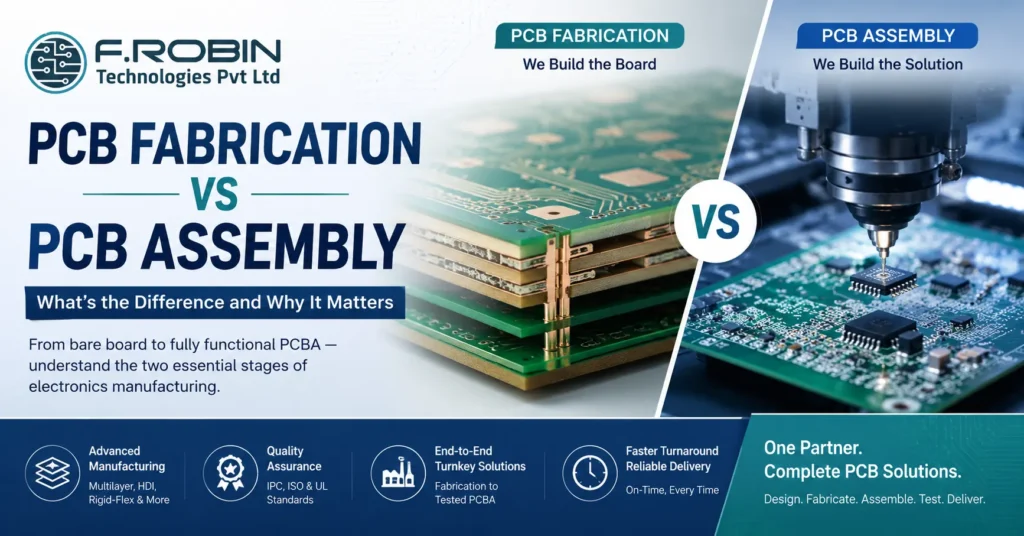
Introduction PCB fabrication vs PCB assembly these two terms appear constantly in electronics manufacturing, often interchangeably and almost always incorrectly. If you have ever sent a quote request to a manufacturer and been unsure whether to ask for “fabrication,” “assembly,” or both, this guide will clear that up completely. In short: fabrication makes the board, while assembly populates it. Together, they produce a functional PCBA. However, the details of each process the different expertise they require, the distinct quality standards they are held to, and the cost implications of each are worth understanding in full, especially if you are about to place your first manufacturing order or are evaluating new suppliers. 1. What Is PCB Fabrication? PCB fabrication is the process of manufacturing the bare printed circuit board — the physical substrate with copper traces, drilled holes, plated vias, solder mask, and silkscreen — but with no components attached. Think of it as building the foundation of a building before any furniture goes in. The board comes out of fabrication as a flat, component-free physical object that carries the electrical connectivity your design requires. Every trace, pad, via, and plane is in place, yet nothing is soldered and nothing is placed. What Happens During PCB Fabrication Preparing the Inner Layers Step 1 — Inner layer imaging (multilayer boards) Copper-clad laminate sheets are coated with photoresist. Next, UV light exposes the circuit pattern onto the resist through a film or laser direct imaging (LDI) system. Unexposed resist is then washed away, and the exposed copper is etched off — leaving only the copper traces of that layer. Step 2 — Lamination For multilayer boards, the individual inner layers are stacked with prepreg (glass-fibre resin sheets) between them and pressed together under heat and pressure in a lamination press. As a result, all layers bond into a single rigid substrate. Step 3 — Drilling CNC drilling machines drill holes through the laminated stack for through-hole component leads, via connections between layers, and mechanical mounting holes. In addition, high-density boards may use laser drilling for microvias where standard CNC cannot reach the required diameter. Step 4 — Plating The drilled holes are electrolessly copper-plated to create electrical conductivity between layers. This plating step is precisely what makes a via a via — a copper-plated barrel connecting two or more copper layers through a drilled hole. Finishing the Board Surface Step 5 — Outer layer imaging and etching Following inner layer processing, the outer copper layers go through the same imaging and etching process, defining the surface traces and pads. Step 6 — Solder mask application A liquid photoimageable solder mask (LPI) is applied over the entire board surface, then exposed and developed to open only the pad areas. Consequently, the traces remain protected by the green (or black, red, or blue) coating you see on a finished PCB, which prevents solder bridging during assembly and protects copper from oxidation. Step 7 — Surface finish The exposed copper pads receive a surface finish to prevent oxidation and ensure good solderability. Common finishes include: Step 8 — Silkscreen printing Reference designators, component outlines, polarity markers, logos, and other markings are printed on the board using white or yellow ink. This silkscreen layer is what your assembler and operators use as a visual reference during assembly and inspection. Step 9 — Electrical testing Every fabricated board is electrically tested — either by flying probe or bed of nails — to verify that all nets are continuous and no unintended shorts exist. Importantly, a board that fails electrical test at fabrication never reaches assembly. Step 10 — Visual inspection, routing, and delivery Finally, boards are inspected visually and under AOI, then routed from the production panel into individual boards or arrays and packaged for delivery. 2. What Is PCB Assembly? PCB assembly (PCBA) is the process of soldering electronic components onto the fabricated bare board to create a functional electronic circuit. Whereas fabrication builds the substrate, assembly populates it. The assembled board — called a PCBA (Printed Circuit Board Assembly) — is the finished functional unit: the thing that goes into your product, gets tested, and performs the electronic function your design was created for. What Happens During PCB Assembly Step 1 — Solder paste stencil printing A laser-cut stainless steel stencil is aligned over the bare board. Solder paste is then squeegeed across the stencil, depositing precise volumes of paste only on the pad areas through the stencil apertures. Critically, paste volume and consistency at this step directly determines solder joint quality downstream. Step 2 — SMT component placement (pick and place) An automated pick-and-place machine retrieves components from reels, trays, and tubes, then places them on the solder-pasted pads with micron-level accuracy. Modern machines handle components as small as 0201 (0.6mm × 0.3mm) and manage fine-pitch BGAs, QFNs, and multi-pin connectors in the same pass. Step 3 — Reflow soldering The populated board travels through a multi-zone reflow oven on a conveyor. Throughout this stage, the temperature profile — preheat, thermal soak, reflow peak, and cooling — is precisely controlled to melt and resolidify the solder paste into reliable intermetallic solder joints without damaging components. Profiles are customised per board based on component thermal sensitivity and paste specification. Step 4: Removed “through-hole components” → replaced with “components” (the step heading already tells the reader it’s through-hole) Step 5: Replaced “Through-hole component leads on the bottom of the board are subsequently soldered” → replaced with “Once insertion is complete, the leads on the bottom of the board are soldered” — breaks the consecutive pattern and adds a transition word Yoast will also count Step 6 — Inspection AOI (Automated Optical Inspection) scans every board for missing components, wrong orientation, solder bridges, lifted leads, and insufficient solder. Additionally, X-ray inspection checks hidden solder joints on BGA and QFN packages, while visual inspection by trained operators provides a final check. Step 7 — Testing Electrical testing (flying probe or ICT) verifies circuit continuity and component values. Furthermore,
