
Turnkey PCB Assembly Services in India: Everything You Need to Know Before Placing an Order
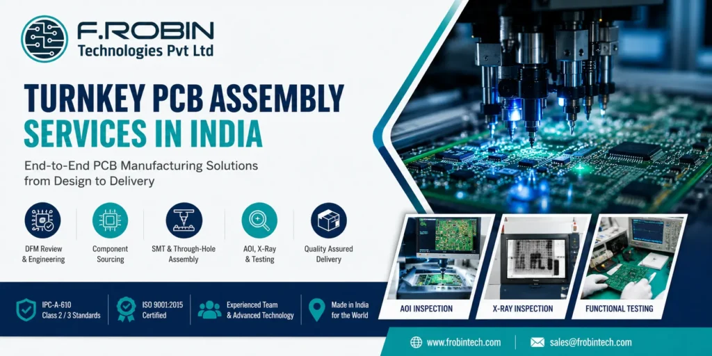
Introduction Turnkey PCB assembly services India are becoming essential for hardware startups, OEMs, R&D teams, and electronics companies looking for reliable PCB manufacturing, component sourcing, SMT assembly, testing, and fast production support under one roof. Whether you are building a prototype, pilot batch, or full production run, choosing the right turnkey PCB assembly partner directly affects product quality, lead times, and manufacturing cost. So you have a PCB design ready. The Gerbers are exported, the BOM is drafted, and you need someone to build it. You search for PCB assembly services in India and are immediately confronted with unfamiliar terms like turnkey, partial turnkey, consignment, PCBA, SMT, AOI, and functional testing. This guide explains everything you need to know before placing an order for turnkey PCB assembly services in India, including the assembly process, testing methods, file preparation, pricing factors, and how to choose the right EMS manufacturing partner. 1. What Are Turnkey PCB Assembly Services in India? Turnkey PCB assembly means you hand off the job completely — design files, BOM, and sometimes the bare PCBs — and receive assembled, tested boards in return. The manufacturer handles component sourcing, procurement, kitting, solder paste printing, pick-and-place, reflow, inspection, and often functional testing. The Three Models Full Turnkey You supply only design files (Gerbers, BOM, centroid file). The manufacturer procures all components, fabricates bare boards, assembles, inspects, and ships finished boards. The most hands-off and most popular option for startups and hardware teams without procurement infrastructure. Partial Turnkey (Kitted Assembly) You supply some components — long-lead items or proprietary parts — and the manufacturer supplies the rest. Common for products with custom ICs, specialised sensors, or parts under NDA. Consignment (CM-Only) You supply everything: bare boards, all components, stencil, sometimes solder paste. The manufacturer provides only assembly labour and equipment. Used by large OEMs with established supply chains. 2. The Turnkey PCBA Process End to End 3. SMT vs Through-Hole Assembly in the Turnkey Context Most modern PCBs are predominantly SMT, but boards with both SMT and through-hole components require understanding the two-pass process. Pure SMT boards are the fastest and most cost-effective to assemble. The entire process is automated. If your design can be fully SMT — using SMD connectors, SMD electrolytic capacitors, SMD crystals — do it. Mixed technology boards (SMT + through-hole) require two passes: SMT components are placed and reflowed first; through-hole components are then inserted and selectively soldered. This adds time and cost, but is often unavoidable for high-current power components and ruggedised connectors. Pure through-hole boards are rare today and are assembled by hand insertion and wave soldering. 4. AOI, X-Ray, and Functional Testing in Turnkey Lines Testing is where many low-cost assemblers cut corners — and where you pay the price when field failures occur. Automated Optical Inspection (AOI) AOI machines use high-resolution cameras and image processing to inspect every solder joint and component placement. AOI catches: What AOI misses: Hidden solder joints (BGA balls, QFN thermal pads), electrical opens/shorts that don’t show optically, and functional failures. X-Ray Inspection X-ray is essential for BGA, QFN, and LGA packages where solder joints are hidden under the component body. It reveals: For any board with a BGA or QFN component, X-ray inspection is mandatory, not optional. In-Circuit Testing (ICT) ICT uses a “bed of nails” fixture with spring-loaded probes contacting test points to measure component values and check for shorts/opens. Fast and thorough but requires a custom fixture costing ₹50,000–₹3,00,000+. Economical only at 500+ units. Flying Probe Testing Flying probe uses movable probes without a custom fixture — ideal for prototype and low-volume runs. Slower than ICT but fixture-free and catches shorts, opens, and component value errors. Functional Testing (FCT) FCT powers up the assembled board and exercises it exactly as in the final product. A custom test jig interfaces with the board’s connectors and I/O, stimulates inputs, and measures outputs. FCT is the only test method that definitively proves the board works. Recommended Testing Strategy by Volume Production Volume Recommended Tests 1–10 Units (Prototype) Visual Inspection + Flying Probe Testing + Functional Circuit Testing (FCT) 10–100 Units (Pilot Run) AOI + X-ray Inspection (for BGA/QFN) + Functional Circuit Testing (FCT) 100–1,000 Units AOI + X-ray Inspection + ICT or Flying Probe Testing + Functional Circuit Testing (FCT) 1,000+ Units (Mass Production) AOI + X-ray Inspection + ICT + Functional Circuit Testing (FCT) + Burn-In Testing 5. Component Sourcing in India — Counterfeit Risk, and Approved Vendor Lists Component sourcing is one of the most overlooked aspects of turnkey assembly — and one of the most consequential. Counterfeit Component Risk Counterfeit electronic components are a real problem, especially sourced through grey-market channels. Counterfeits can fail immediately, pass initial testing and fail in the field, or cause safety issues. To mitigate risk: Approved Vendor Lists (AVL) An AVL is a list of approved manufacturers and distributors for each BOM line item. For prototype runs, authorised distributors are sufficient. For production, define and submit your AVL with your production BOM. 6. How to Prepare Files for Turnkey Assembly Poor file preparation is the single most common cause of delays, miscommunications, and assembly errors. Gerber Files (RS-274X Format) Include: all copper layers, solder mask layers (top and bottom), silkscreen layers, drill file (Excellon format), and board outline. Name layers clearly. Double-check: Bill of Materials (BOM) Every component must include: A BOM with only generic descriptions (“100nF capacitor, 0402”) forces sourcing assumptions that may not match your design intent. Always provide MPNs. Centroid / Pick-and-Place / XY File Contains reference designator, X and Y coordinates, rotation angle, and board side for every SMT component. Export from your PCB tool and verify the coordinate origin matches your Gerber origin. A mismatch causes your assembler to manually adjust every component location. Assembly Drawing A 2D PDF showing top and bottom of the assembled board with reference designators visible, polarity markings for diodes and electrolytic capacitors, and any special assembly notes. Test Specification (for FCT) Describe what the board must do, how
