
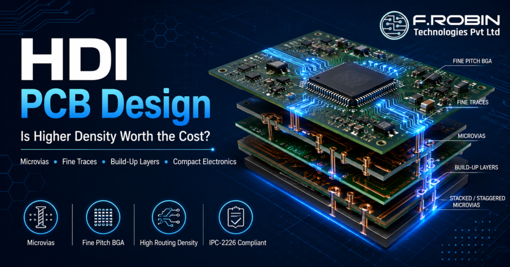
High density interconnect (HDI) PCB design packs more circuitry into less space than a conventional board, using microvias, finer traces, and tighter spacing. As electronics shrink and components grow more complex, HDI has moved from a niche option to a mainstream necessity. But it also costs more — so the real question is whether high-density design is worth it for your product.
This guide explains HDI PCB design in plain terms: what it is, the key technologies behind it, when it pays off, and the design rules that keep it reliable. Whether you are designing a compact wearable or a dense processor board, you will learn when a high density interconnect approach is the right call.
What Is HDI PCB Design?
High density interconnect PCB design is an approach that achieves higher wiring density than standard boards through microvias, fine lines, and thin build-up layers. In short, it lets you route far more connections in the same area — or fit the same circuit into a much smaller board.
An HDI circuit board uses laser-drilled microvias instead of large mechanically drilled holes, along with finer traces and tighter spacing. These features free up routing space that conventional vias would block. As a result, a high density interconnect PCB can support today’s fine-pitch components, which a standard board often cannot.
HDI is defined by IPC-2226, which classifies designs into types based on their build-up structure. The common thread is the same: more connections, smaller features, and a board built up in layers rather than drilled all at once.
HDI vs Standard PCB Design
The difference between HDI and a standard board comes down to density and how the board is built. A conventional PCB is drilled and plated in a single pass with through-hole vias. A high density interconnect PCB is built up in stages, adding thin layers with microvias between them.
This staged construction unlocks much greater density. Where a standard board hits a routing wall, HDI keeps going — fanning out hundreds of pins from a fine-pitch BGA that through-holes could never escape. The trade-off is added cost and manufacturing complexity, which we cover below.
For designs that are not space-constrained, a conventional multilayer PCB usually offers better value. HDI earns its place only when density genuinely demands it.
Key HDI Technologies
Several technologies make high density interconnect design possible. Understanding them clarifies what HDI actually involves.
- Microvias. Tiny laser-drilled vias connecting adjacent layers — the foundation of HDI.
- Via-in-pad. Vias placed directly in component pads to save space under fine-pitch parts.
- Stacked and staggered vias. Microvias arranged across multiple layers to route through the build-up.
- Build-up layers. Thin dielectric and copper layers added over a core in sequence.
- Fine traces and spacing. Narrower lines that pack more routing into each layer.
These work together to escape dense components. A fine-pitch BGA, for example, may need via-in-pad and stacked microvias just to break out every signal. For a closer look at the via economics, see our guide to blind and buried vias.
When Does HDI Pay Off?
High density interconnect design pays off when density, size, or performance demands exceed what a standard board can deliver. It is worth the investment when:
- You use fine-pitch BGAs with pin counts that through-holes cannot escape.
- Space is tight, as in phones, wearables, medical, and IoT devices.
- High layer counts would otherwise be needed to route a dense design.
- Signal integrity matters, since shorter microvia paths reduce stubs and improve high-speed performance.
- Miniaturization wins markets, and a smaller, lighter board is a competitive edge.
In these cases, a high density interconnect approach is not optional — the product could not exist, or would be far larger, without it. That is when the extra cost is clearly justified.
HDI Design Rules
Reliable high density interconnect boards follow a set of core design rules. Respecting them keeps the board manufacturable and robust.
- Microvia aspect ratio. Keep the microvia depth-to-diameter ratio within your fab’s limits (commonly around 1:1).
- Capture and target pads. Size pads correctly for laser drilling and plating.
- Stack-up planning. Define the build-up structure (IPC-2226 Type I, II, or III) early, as it governs the whole design.
- Via-in-pad filling. Fill and cap via-in-pad so the surface stays flat and solderable.
- Layer transitions. Plan how signals move through stacked or staggered microvias.
Following these rules — and the IPC-2226 standard — prevents the most common HDI failures. Designing within your manufacturer’s stated capabilities is just as important as the rules themselves.
HDI Build-Up Types (IPC-2226)
IPC-2226 classifies high density interconnect boards by their build-up structure, which helps you and your fabricator agree on complexity:
- Type I. A single microvia layer on one or both sides of a core — the simplest, lowest-cost HDI.
- Type II. Microvias plus buried vias in the core, adding routing capacity.
- Type III. Two or more microvia layers per side, stacked or staggered, for the densest designs.
As the type number rises, so does density — and cost. Choosing the lowest type that meets your routing needs is the single biggest lever for keeping an HDI board affordable. Discuss the target type with your fabricator before you finalize the stack-up, since it shapes every later decision.
Cost Considerations
HDI costs more than standard PCB design, mainly because of how it is built. Sequential lamination, laser drilling, and tighter tolerances each add process steps, time, and inspection.
As a rule, every added build-up layer or lamination cycle raises cost. So the smart approach is to use the minimum HDI complexity that meets your needs — not the most advanced structure available. A clean handoff to PCB manufacturing keeps those costs predictable, and your fabricator can advise which HDI type balances density and price for your board.
Best Practices for HDI Design
Apply these practices to get the most from a high density interconnect design:
- Use only the HDI complexity you need. Match the build-up to real density, not ambition.
- Plan the stack-up first, since via structures depend on it.
- Coordinate early with your fab on microvia size and aspect ratio.
- Design via-in-pad correctly, with proper filling and capping.
- Follow IPC-2226 for reliable, manufacturable HDI.
Sound HDI design balances density, reliability, and cost. Working with experienced PCB layout design services helps you adopt only the high density interconnect features your product truly requires.
Common Mistakes to Avoid
Even capable teams trip up on HDI. Watch for these:
- Over-engineering the board with HDI a design does not need.
- Ignoring fab capabilities for microvia size and aspect ratio.
- Planning the stack-up too late, after routing has started.
- Skipping via-in-pad filling, causing solder defects.
- Forgetting IPC-2226 classification, leading to unmanufacturable structures.
Avoiding these keeps your high density interconnect board reliable, manufacturable, and on budget.
Key Takeaways
- High density interconnect (HDI) PCB design packs more circuitry into less space using microvias and fine features.
- HDI is built up in layers, unlike a standard board drilled in one pass.
- Key technologies: microvias, via-in-pad, stacked/staggered vias, and build-up layers.
- HDI pays off for fine-pitch BGAs, tight spaces, high layer counts, and high-speed signals.
- It costs more, so use the minimum complexity that meets your needs.
- Follow IPC-2226 design rules and your fab’s capabilities.
Conclusion
HDI PCB design is worth it when your product’s density, size, or performance demands exceed what a standard board can deliver — fine-pitch BGAs, tight spaces, high layer counts, or high-speed signals. A high density interconnect approach uses microvias, via-in-pad, and build-up layers to achieve that density, at higher cost. The key is matching the HDI complexity to your real needs and following IPC-2226 design rules.
Frequently Asked Questions
1. What is HDI PCB design?
HDI (High Density Interconnect) PCB design achieves higher wiring density than standard boards using microvias, fine traces, and thin build-up layers, allowing more connections in less space.
2. What is a high density interconnect PCB?
A high density interconnect PCB is a board built with laser-drilled microvias, fine traces, and sequential build-up layers to support fine-pitch components and compact electronic designs.
3. What is the difference between HDI and a standard PCB?
A standard PCB primarily uses through-hole vias, whereas an HDI PCB uses microvias, finer traces, and advanced layer stacking to achieve significantly higher routing density and improved electrical performance.
4. When is HDI PCB design worth it?
HDI PCB design is ideal for fine-pitch BGAs, compact products, high-speed circuits, and applications requiring high routing density without increasing board size.
5. What are microvias?
Microvias are tiny laser-drilled vias that connect adjacent PCB layers. They are a key technology in HDI PCB design, enabling reliable routing for high-density electronic assemblies.
