

Multilayer PCB design best practices are what separate boards that pass EMC testing and work reliably in the field from those that don’t. As signals run faster, components shrink smaller, and certification requirements grow stricter, getting the fundamentals right before layout begins has never been more critical.
This guide walks you through 10 proven best practices — from stackup planning and impedance control to thermal management and DFM so your multilayer design gets it right before a single Gerber file is sent to fabrication.
What Is Multilayer PCB Design?
Multilayer PCB design is the process of creating printed circuit boards with three or more copper layers separated by dielectric (insulating) materials, laminated under heat and pressure into a single rigid structure.
Each layer serves a dedicated purpose signal routing, power distribution, or ground reference — enabling engineers to pack far more functionality into a smaller board footprint than single- or double-layer designs allow.
Multilayer PCBs are the foundation of virtually every high-performance electronic product today: smartphones, industrial controllers, medical imaging equipment, 5G base stations, automotive ECUs, and aerospace avionics all rely on them.
When Does a Design Need More Than Two Layers?
Not every board needs to be multilayer. However, your design almost certainly does if it includes any of the following:
- High-speed digital signals (USB, PCIe, HDMI, DDR, Gigabit Ethernet)
- A dense component footprint with limited routing space on two layers
- EMC requirements that a two-layer board cannot meet
- Mixed analog and digital circuits that need domain isolation
- Fine-pitch BGA or QFN components requiring dense via escape routing
- Controlled impedance requirements (typically 50 Ω single-ended, 90–100 Ω differential)
- Multiple power rails needing dedicated plane layers
If any of these apply, the question is no longer whether to go multilayer it’s how many layers and how to structure them. That’s exactly what the following best practices cover.
Best Practice 1 — Plan Your Layer Stackup First
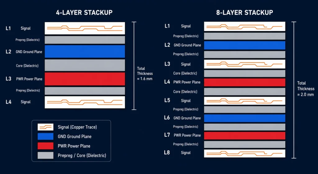
The stackup is the architectural blueprint of your multilayer PCB. It defines the number of layers, their sequence, the dielectric material between them, and the copper thickness on each layer.
Plan your stackup before routing a single trace. Every impedance calculation, every signal layer assignment, and every power plane decision flows from it. Changing the stackup mid-layout invalidates every impedance-controlled trace and forces expensive re-routing.
Key Stackup Principles
- Maintain symmetry. Balance the stackup around the board’s centre to prevent warping during reflow and lamination. In an 8-layer board, mirror signal and plane layers around the centre axis.
- Always place a ground plane adjacent to every signal layer. This provides a controlled impedance reference and a short return path for signal currents.
- Separate power planes from signal layers with a ground plane between them. Never place two high-current power planes directly adjacent to each other.
- Keep high-speed signal layers close to their reference planes. Both microstrip (outer layer) and stripline (inner layer) geometries rely on the proximity of a reference plane to achieve controlled impedance.
Standard Stackup Reference
| Layer Count | Typical Arrangement | Best For |
|---|---|---|
| 4-layer | Signal / GND / PWR / Signal | Medium-density microcontrollers, IoT, industrial |
| 6-layer | Signal / GND / Signal / Signal / PWR / Signal | RF segregation, additional routing space |
| 8-layer | Signal / GND / Signal / GND / PWR / Signal / GND / Signal | DDR, PCIe, multi-power-rail SoC designs |
| 12+ layer | Complex alternating signal/plane | Advanced FPGA, telecom, aerospace |
Best Practice 2 — Choose the Right Layer Count
More layers are not always better. Each additional layer adds fabrication cost, increases board thickness, and complicates via drilling and lamination. Too few layers, however, force routing compromises that degrade performance and EMC behaviour.
How to Choose the Right Layer Count
- Estimate routing density first.
Calculate your total net count and available routing channels. If two layers cannot accommodate clean routing, move to four before considering more.
- Count your power rails.
Each major voltage domain benefits from its own power plane. Four separate rails on a four-layer board is already tight.
- Consider your highest-frequency signal.
For signals above 100 MHz, inner stripline layers sandwiched between ground planes are strongly preferred for EMI shielding.
- Factor in manufacturing cost.
Layer count is one of the largest cost drivers in PCB fabrication. Ask your manufacturer for comparative pricing at your target count versus one layer higher the delta is often smaller than expected for the reliability gain you receive.
Best Practice 3 — Master Signal Integrity and Impedance Control
Signal integrity (SI) is the discipline of ensuring signals propagate accurately without distortion, ringing, or reflections. In multilayer PCB design, SI is controlled primarily through impedance management.
What Is Controlled Impedance?
Controlled impedance means designing trace geometry width and thickness — alongside dielectric thickness so that the characteristic impedance of a trace matches the system impedance. Typical targets:
- 50 Ω for single-ended signals (USB, SPI, UART at high speeds)
- 90–100 Ω differential for USB 2.0 and 3.0, HDMI, PCIe
- 100 Ω differential for Ethernet
How to Achieve Controlled Impedance
- Use an impedance calculator most EDA tools include one with your exact stackup dimensions and the dielectric constant (Dk) of your chosen laminate.
- Specify impedance requirements clearly in your fabrication notes: for example, “50 Ω ±10% on Layer 1 microstrip, reference Layer 2 GND.”
- Work with your PCB fabricator to confirm their process can hold the specified tolerance. Standard is ±10%; tight is ±5%.
- For DDR, PCIe, or SERDES interfaces, request a pre-production impedance test coupon from your manufacturer.
Best Practice 4 — Use Solid Ground Planes and Manage Return Paths
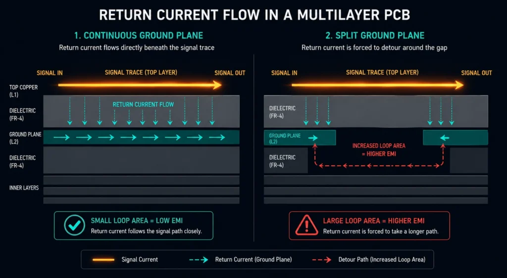
The ground plane is not just a reference potential it is an active participant in signal transmission. Return current travels in the ground plane directly beneath a signal trace, following the path of least inductance, not least resistance.
Ground Plane Best Practices
- Never split a ground plane under a high-speed signal trace. A split forces return current to take a long looping path around the gap, dramatically increasing loop area and EMI emissions.
- Use a single, unified ground plane for digital circuits wherever possible. Do not split the plane under shared signals.
- Place ground vias near every power pin and decoupling capacitor. Short, direct paths from component ground pins to the plane reduce parasitic inductance.
- Add a ground via whenever a signal transitions to a different layer. The return current must also change layers at that point — a nearby ground via provides the path it needs.
Per the IPC- 2221 generic requirement of the design, maintaining continuous ground reference planes is a fundamental requirement for reliable high-speed multilayer PCB designs.
Best Practice 5 — Route High-Speed Signals on Inner Layers
Inner signal layers use a stripline geometry — the trace is sandwiched between two reference planes, which confine the electric field to the dielectric and provide natural EMI shielding on both sides.
When to Use Inner vs. Outer Layers
| Signal Type | Recommended Layer | Reason |
|---|---|---|
| Clock, DDR, PCIe, high-speed bus | Inner (stripline) | Shielded between reference planes; lower EMI |
| Low-speed I/O, LED control, power signals | Outer (microstrip) | Easy access; EMI not critical |
| RF / antenna traces | Outer with controlled reference distance | Specific impedance and radiation requirements |
| Differential pairs (USB, HDMI, Ethernet) | Inner preferred, outer acceptable | Keep pairs on same layer; minimise layer changes |
Keep differential pairs on the same layer throughout their entire route. Every layer change via is an impedance discontinuity. If a layer change is unavoidable, use matched-length via stubs and place the transition well away from connectors and receivers.
Best Practice 6 — Control Crosstalk With Layer Routing Direction
Crosstalk is unwanted signal coupling between adjacent traces. In multilayer PCBs, the risk is highest between parallel traces on adjacent signal layers.
The Perpendicular Routing Rule
Route adjacent signal layers perpendicular to each other:
- Layer 1 (Top Signal): route traces horizontally
- Next signal layer: route traces vertically
This perpendicular relationship minimises the length over which traces on adjacent layers run parallel, dramatically reducing both capacitive and inductive coupling between them.
Additional Crosstalk Reduction Techniques
- Maintain trace-to-trace spacing of at least 3× the trace width (3W rule) for critical signals.
- For clock and high-frequency signals, use a guard trace a grounded trace on either side of the critical signal on the same layer.
- Route differential pairs with tightly controlled, consistent spacing matched to the differential impedance specification throughout the entire route.
Best Practice 7 — Choose and Place Vias Strategically
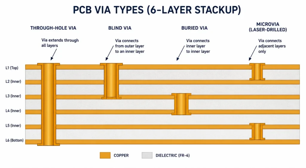
Vias are the vertical interconnects between layers. Via selection and placement directly affect routing density, signal quality, and manufacturing cost.
Via Types in Multilayer PCBs
| Via Type | Description | Best Use |
|---|---|---|
| Through-hole via | Drilled through all layers | Standard inter-layer connections; lowest cost |
| Blind via | Connects outer layer to one or more inner layers only | BGA escape routing; saves routing space on unused layers |
| Buried via | Connects two inner layers only; not visible from outside | Ultra-high-density designs; higher fabrication cost |
| Microvia (laser-drilled) | ≤0.15 mm diameter; HDI boards only | Fine-pitch BGA (0.5 mm pitch and below) |
Via Placement Best Practices
- Avoid via stubs on high-speed signals. A through-hole via used only for Layers 1–2 leaves an unused stub on Layers 3–4 that creates signal reflections at GHz frequencies. Use back-drilling or blind vias to eliminate stubs.
- Place decoupling capacitors as close as possible to power vias. Via inductance between the capacitor and the power pin degrades decoupling effectiveness at high frequencies.
- Avoid vias directly under BGAs unless the design specifically uses via-in-pad which requires tenting or filling to prevent solder wicking during reflow.
- Cluster ground vias near power vias to form tight, low-inductance decoupling loops.
Best Practice 8 — Manage Thermal Distribution Across Layers
Heat is one of the leading causes of field failures in electronics. Thermal management in multilayer PCBs must be designed in from the start — not added as a retrofit after layout is complete.
Thermal Management Best Practices
- Use thermal vias to conduct heat to inner copper pours. Arrays of small, copper-filled vias beneath high-dissipation components transfer heat from the top surface down to inner plane layers that act as heat spreaders.
- Place high-dissipation components away from thermally sensitive devices. Keep power regulators, motor drivers, and RF power amplifiers away from precision ADCs, oscillators, and sensors.
- Increase copper weight on high-current power layers. Standard copper weight is 1 oz/ft²; specify 2 oz or heavier for traces or planes carrying more than 3–5 A continuously.
- Run thermal simulation before fabrication. Tools like Cadence Allegro, Altium Designer, and Cadence’s PCB design suite support thermal simulation. A simulated hot spot is far cheaper to fix than one discovered during reliability testing.
Best Practice 9 — Separate Analog and Digital Domains
Mixing analog and digital circuits on the same multilayer board sensors, ADCs, audio, RF alongside digital processors and memory is one of the most challenging aspects of multilayer PCB design. Digital switching noise couples readily into sensitive analog signals if the two domains are not carefully separated.
Domain Separation Strategy
- Physically partition the board. Place analog components on one side or corner; digital components on the other. Do not interleave them.
- Route analog signal traces over the analog ground region. Never route a digital signal trace over an analog section of the ground plane.
- Use a single, unified ground plane for most mixed-signal designs. Keep all analog signal routing physically above the analog region of the ground plane to ensure clean, short return paths.
- Place ADCs and DACs at the boundary between analog and digital regions, with their analog pins facing the analog section and their digital pins facing the digital section.
- Use ferrite beads or LC filters to isolate analog power supplies from digital power supplies, even when they share the same voltage level.
Best Practice 10 — Design for Manufacturability From Day One
The best electrical design fails if it cannot be manufactured reliably and economically. DFM in multilayer PCBs means applying your fabricator’s process constraints throughout layout not checking them at the end.
Critical DFM Checks for Multilayer PCBs
- Minimum trace/space: Confirm your fabricator’s capability typically 3–4 mil for standard processes, 2 mil for advanced. Design 20% above their minimum for yield reliability.
- Drill-to-copper clearance: Maintain adequate annular ring on all via pads to survive drill registration tolerances in production.
- Aspect ratio: The ratio of board thickness to drill diameter. Standard maximum is 8:1 to 10:1. Exceeding this causes plating failures in deep vias.
- Symmetric copper distribution: Balance copper coverage across layers to prevent differential thermal expansion during lamination, which causes warping.
- Solder mask web: Leave adequate solder mask web between SMD pads on fine-pitch components to prevent bridging during reflow.
- Via-to-pad clearance: Do not place vias inside or too close to SMT pads unless using via-in-pad with proper fill and planarisation.
Submitting your multilayer design for a professional DFM review before fabrication catches these issues before they become costly yield problems. Our PCB assembly services include a full DFM review with every order.
The IPC-A-600 Acceptability of Printed Boards standard defines the acceptability criteria your fabricated board will be evaluated against. Designing to those criteria upfront avoids rejection at incoming inspection.
Common Multilayer PCB Design Mistakes to Avoid
Even experienced engineers make these errors. Catching them early saves significant time and cost.
- Changing the stackup after routing has begun. This invalidates every impedance-controlled trace and forces partial or full re-routing. Lock the stackup before placing a single component.
- Splitting a ground plane under a high-speed trace. Return currents can no longer follow the signal trace, causing EMI failures and signal integrity degradation.
- Ignoring via stubs on high-speed interfaces. Stubs create reflections that degrade signal quality at GHz frequencies. Use back-drilling or blind/buried vias to eliminate them.
- Routing differential pairs across layer transitions without matched vias. Asymmetric via placement causes phase mismatch and common-mode noise injection.
- Under-specifying the fabrication notes. Missing impedance targets, copper weight callouts, or IPC class designations leads the manufacturer to make assumptions often wrong ones.
- Skipping a pre-production DFM review. A fabricator’s DFM review catches process-specific issues your EDA design rules cannot know about.
Work With F.Robin Technologies on Your Next Multilayer Design
Applying these multilayer PCB design best practices reduces EMC failures, improves signal integrity, and gets your board through fabrication first time. However, knowing the rules and executing them under real project constraints are two different things.
At F.Robin Technologies, our engineering team provides:
- Full multilayer PCB layout and design — from stackup planning through Gerber file generation
- HDI and controlled impedance designs verified against your fabricator’s process capabilities
- Signal integrity analysis for high-speed interfaces — PCIe, DDR, SERDES, LVDS, and more
Start Your Next Multilayer PCB Design With Confidence
Whether you are starting a new design or troubleshooting an existing layout, our engineering team is ready to help with stackup planning, impedance control, signal integrity analysis, HDI routing, and manufacturable multilayer PCB layouts.
Contact F.Robin Technologies →FAQs
It depends on design complexity. A 4-layer board handles most medium-density microcontroller and IoT designs well. High-speed interfaces like DDR4, PCIe Gen4, or dense FPGA designs typically need 8–12 layers. Choose the layer count that provides adequate routing space and proper power/ground plane coverage for your specific design.
A solid ground plane provides a controlled impedance reference for signal traces, a low-inductance return path for signal currents, and an EMI shield between signal layers. Broken or split ground planes are one of the most common root causes of EMI failures and signal integrity problems in multilayer designs.
Controlled impedance means manufacturing a PCB so that specific traces have a defined characteristic impedance — typically 50 Ω single-ended or 100 Ω differential. This is achieved by controlling trace width, copper thickness, and dielectric thickness in the stackup. It is essential for high-speed digital interfaces like USB, PCIe, DDR, and Ethernet.
The 3W rule states that the edge-to-edge spacing between parallel signal traces should be at least 3 times the trace width. This minimum spacing reduces capacitive coupling (crosstalk) between adjacent traces. For critical signals such as clocks and high-speed buses, apply the 3W rule as a minimum, not a target.
