

Introduction
Every electronic device you use — from your smartphone to an industrial robot runs on a printed circuit board. PCB design is the engineering process that makes this possible.
Whether you’re a student, startup founder, or product designer, this guide walks you through the complete PCB design process — from basics to best practices.
What Is PCB Design?
PCB design is the process of turning an electrical schematic into a physical, manufacturable circuit board. It involves placing components, routing copper traces, and generating Gerber files for fabrication. A PCB connects electronic parts mechanically and electrically using copper traces on a non-conductive base like FR-4 fiberglass.
Why PCB Design Matters
A well-designed PCB board directly affects product performance, reliability, and cost. Here’s why it matters:
- Signal integrity — proper routing reduces noise and reflections
- Thermal management — smart placement dissipates heat efficiently
- EMI compliance — good layout prevents electromagnetic interference
- Manufacturability — DFM practices reduce production errors
- Cost control — fewer layers and efficient routing lower unit cost
The PCB Design Process — Step by Step
- Schematic Capture
Define all components and their connections using schematic symbols in tools like KiCad or Altium Designer.
- Footprint Assignment
Assign each component a physical footprint — its solder pads and body dimensions on the board.
- Layer Stackup Definition
Choose the number of copper layers and material. Most basic boards use 2 layers; complex designs use 4–8+.
- Component Placement
Position components on the board. Keep signal paths short, separate analog and digital sections, and follow enclosure constraints.
- Trace Routing
Connect all components with copper traces. Set correct trace widths based on current load using IPC-2221 standards.
- Design Rule Check (DRC)
Run an automated DRC to catch errors — clearance violations, unconnected nets, and silkscreen overlaps
- Gerber File Export
Export Gerber files — the industry-standard format PCB manufacturers use to fabricate your board.
PCB Design Process — Quick Reference Table
| Stage | Activity | Output |
| Schematic Capture | Draw circuit logic | Netlist |
| Footprint Assignment | Link components to pads | BOM + footprints |
| Layer Stackup | Define layers and materials | Stackup spec |
| Component Placement | Position parts on board | Placed layout |
| Trace Routing | Route all copper connections | Routed PCB |
| DRC | Validate design rules | Clean DRC report |
| Gerber Export | Generate fabrication files | Gerber + drill files |
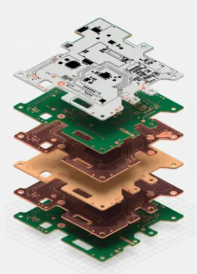
PCB Board Design — Layers and Materials
| Layer | Purpose | Material |
| Top/Bottom Copper | Signal routing, component pads | 1–2 oz copper foil |
| Inner Copper | Power and ground planes | 0.5–2 oz copper |
| Soldermask | Protects copper from solder bridges | LPI epoxy |
| Silkscreen | Component labels | Epoxy ink |
| Core / Prepreg | Dielectric base between layers | FR-4 fiberglass |
Standard substrate: FR-4 fiberglass for most designs. RF/Microwave designs: Rogers 4003C or Taconic TLY for lower signal loss.
PCB Layout Design Best Practices
Power and Ground Planes
- Use dedicated inner layers for power and ground
- Place decoupling capacitors directly at IC power pins
- Avoid splitting ground planes
Signal Routing
- Use 45° bends — never 90° corners
- Match lengths on differential pairs
- Keep high-speed traces away from board edges
Thermal Management
- Place thermal vias under high-power components
- Add thermal relief on through-hole pads connected to ground planes
Top PCB Design Tools in 2026
| Tool | Best For | Cost |
| Altium Designer | Professional / enterprise | ~$10K/yr |
| KiCad | Students, startups, open-source | Free |
| Cadence Allegro | High-speed, complex SoC boards | Enterprise |
| Autodesk Eagle | Hobbyists, Fusion 360 users | Subscription |
| EasyEDA | Beginners, fast prototyping | Free |
Common PCB Design Mistakes to Avoid
| Mistake | How to Fix |
| Skipping impedance planning | Define controlled-impedance nets early |
| Poor decoupling capacitor placement | Place 100nF cap directly at every IC power pin |
| Floating copper pours | Connect all copper fills to GND or PWR net |
| Silkscreen overlapping pads | Run silkscreen DRC check before export |
| Ignoring annular ring rules | Check fab house minimums; use via wizard |
Conclusion
PCB design is the foundation of every electronic product. Whether you’re building a 2-layer prototype or a complex 8-layer high-speed board, the fundamentals stay the same — clean schematic, smart placement, careful routing, and DRC validation before fabrication.
Start with KiCad, follow IPC standards, and build your skills one project at a time.
Ready to Bring Your PCB Design to Life?
Designing a PCB is just the first step — getting it built right is where most teams struggle. Frobin Tech handles the complete PCB design process, from schematic capture and component selection to multilayer layout, DFM review, and fabrication-ready Gerber files.
Whether you’re a hardware startup launching your first product or an engineering team looking for a reliable PCB design partner, Frobin Tech is ready to help.
Get a Free PCB Design ConsultationFAQ
PCB design is the process of converting an electrical schematic into a physical, manufacturable circuit board layout.
Seven stages: schematic capture → footprint assignment → layer stackup → component placement → trace routing → DRC → Gerber export.
KiCad — free, open-source, full-featured, and accepted by all major PCB fabricators.
Beginners can learn the basics in 3–6 months using KiCad. Professional-level skills take 2–4 years of hands-on experience
Gerber files are the standard output format from PCB design software. Manufacturers use them to fabricate the physical board.
PCB design is the full end-to-end process. PCB layout design refers specifically to the component placement and trace routing phase.
