
Types of PCB Manufacturing Process: A Complete Guide for Engineers and Buyers
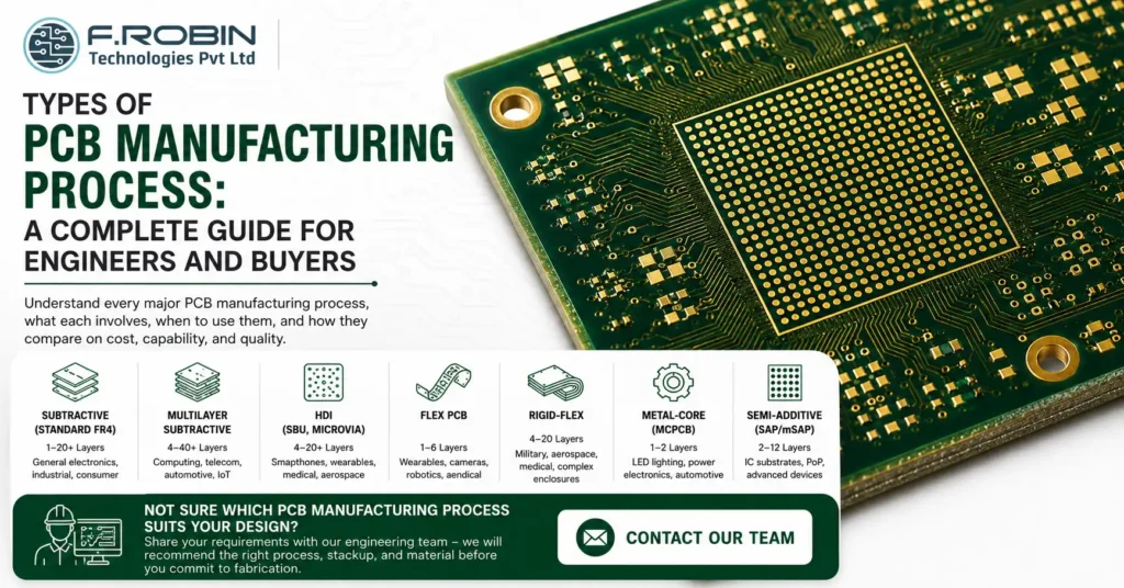
Introduction The types of PCB manufacturing process determine everything downstream board complexity, layer count, material choice, cost, lead time, and the electrical performance of the finished board. Yet for most hardware teams, the manufacturing process is a black box: you send Gerbers, you receive boards. Understanding what actually happens inside that black box — and which process applies to which board type helps you make better design decisions, write more accurate specifications, choose the right fabricator, and avoid costly surprises at the DFM stage. In this guide, we cover every major PCB manufacturing process type, what each involves, when each is appropriate, and how they compare on cost, capability, and quality. 1. The Core PCB Manufacturing Process Subtractive Fabrication The most widely used PCB manufacturing process globally is subtractive fabrication also called the subtractive method or print-and-etch process. It is the standard process for the vast majority of FR4 rigid PCBs manufactured today, from single-layer boards to complex multilayer designs. How the subtractive process works The subtractive process starts with a copper-clad laminate a fibreglass substrate (FR4) with copper foil bonded to one or both sides. The unwanted copper is selectively removed through a sequence of imaging, etching, and plating steps, leaving behind only the copper traces, pads, and planes defined by the design. Preparing the Inner Layers Step 1 — Photolithography (inner layer imaging) The copper surface is coated with a light-sensitive photoresist. A photomask or in modern facilities, a laser direct imaging (LDI) system exposes the circuit pattern onto the resist. Consequently, the unexposed resist is washed away, and the exposed copper underneath is chemically etched off. What remains is precisely the copper circuit pattern of that layer. Step 2 — Lamination For multilayer boards, the individual inner layers are stacked with prepreg (glass-fibre epoxy resin sheets) between them and bonded under heat and pressure in a hydraulic lamination press. As a result, all layers fuse into a single rigid, uniform substrate. Step 3 — Mechanical and laser drilling CNC drilling machines create holes for through-hole component leads, via connections between copper layers, and mechanical mounting points. In addition, high-density boards use laser drilling to create microvias holes too small for mechanical drills, typically under 150µm in diameter. Finishing the Board Step 4 — Through-hole plating The drilled holes are copper-plated by electroless deposition followed by electrolytic plating, creating a conductive copper barrel through the hole that electrically connects layers. This step is fundamentally what distinguishes a multilayer PCB from a simple stack of copper sheets. Step 5 — Outer layer imaging and etching Following plating, the outer copper layers go through the same photolithography and etching process as the inner layers, defining the surface traces, pads, and planes. Step 6 — Solder mask, surface finish, and silkscreen A liquid photoimageable solder mask (LPI) is applied and cured, opening only the pad areas. A surface finish (HASL, ENIG, OSP, or hard gold) is applied to exposed pads. Finally, reference designators and component outlines are printed as silkscreen. Step 7 — Electrical test and delivery Every board is electrically tested by flying probe or bed of nails before shipment, verifying continuity and absence of shorts. The subtractive process is cost-effective, mature, and supported by every PCB fabricator in India and globally. For standard FR4 rigid boards — single layer through to 20+ layers it remains the default manufacturing method. 2. Multilayer PCB Manufacturing Process Multilayer PCB manufacturing follows the same subtractive process as single and double-sided boards, but adds repeated lamination cycles to build up the layer stack. It is the dominant process for all complex, high-density electronic designs. What makes multilayer manufacturing different Layer count options Multilayer boards are built in even numbers of layers: 4, 6, 8, 10, 12, and up to 40+ layers for advanced computing and telecommunications hardware. Each additional pair of layers adds one lamination cycle, drilling pass, and plating step. Inner Layer Processing Core fabrication Each inner layer starts as a separate copper-clad core a rigid substrate with copper on both sides. The circuit pattern is imaged and etched onto each core individually before the stack is assembled. Crucially, inner layers cannot be reworked after lamination, so imaging yield at this stage must be near-perfect. Prepreg and stackup Between each core, sheets of prepreg (B-stage epoxy glass) are placed. The stackup sequence which layers are signal, power, or ground is defined by the designer and must be communicated to the fabricator in the stackup specification. Signal integrity, controlled impedance, and EMI performance all depend on correct stackup execution. Via Types in Multilayer Boards Through-hole vias pass from the top surface to the bottom surface through all layers. They are drilled after lamination and plated in a single pass the most common and least expensive via type. Blind vias connect an outer layer to one or more inner layers without passing all the way through the board. They require sequential lamination laminating a partial stack, drilling and plating, then laminating further layers on top. Buried vias connect two or more inner layers without reaching either outer surface. They are drilled and plated before lamination and are invisible in the finished board. Microvias are laser-drilled vias with diameters typically below 150µm, used in HDI (High-Density Interconnect) designs. They enable very high component density by connecting adjacent layers over a very short distance. Multilayer PCB manufacturing requires tighter process control than single or double-sided boards because registration errors between layers compound with each added layer. For a 12-layer board, the inner layer alignment tolerance must be held across 10 separate imaging and etching cycles. 3. HDI PCB Manufacturing Process (High-Density Interconnect) HDI PCB manufacturing is a specialised extension of multilayer fabrication designed for boards with extremely high component density smartphones, wearables, advanced IoT modules, medical implants, and aerospace electronics. What defines HDI manufacturing HDI boards are characterised by line widths and spaces below 100µm, via diameters below 150µm (microvias), via-in-pad structures, and sequential build-up (SBU) lamination. As a result, they achieve far greater routing density
