PCB Design & Layout
PCB design and layout is the foundation of every reliable electronic product. It is the process of arranging components and routing electrical connections on a printed circuit board to achieve the best signal integrity, thermal performance, and manufacturability.
At F.Robin Technologies, we offer end-to-end PCB design services built around precision and performance. Our experienced engineers combine deep technical knowledge with advanced EDA tools — delivering PCB board design solutions that excel in reliability, scalability, and compliance.
Whether you need a compact flexible PCB design, a high-speed PCB design for RF or networking applications, or a PCB multilayer stackup for complex mixed-signal systems — we deliver accuracy from the first PCB schematic design to the final Gerber file.
From concept to production, our proven PCB layout design method ensures your product reaches market faster, with fewer redesign cycles and zero compromise on quality — backed by our in-house PCB manufacturing capabilities. Partner with F.Robin Technologies for next-generation PCB board layout and design solutions that meet the highest industry standards.
Why F.Robin Technologies?
Decades of Expertise
Our senior PCB layout engineers have served critical industries including aerospace, automotive, medical electronics, and industrial automation — where precision and reliability are non-negotiable.
Advanced Tools
We use industry-leading EDA platforms including Altium Designer and Cadence Allegro ensuring optimal signal integrity, DRC compliance, and design-for-manufacturability from day one.
Custom Solutions
We design tailored PCB layouts that meet your exact specifications whether it's a simple 2-layer prototype or a complex 6-layer high-speed board with tight impedance control requirements.
Complete Support
Our support covers the full PCB design lifecycle from schematic capture and component placement to DFM review, simulation, and production-ready file delivery. .
Our Core Competencies
High-Speed PCB Design
We apply controlled impedance routing, differential pair matching, and crosstalk minimization to ensure signal integrity at frequencies above 1 GHz. Our high-speed PCB design expertise covers networking, RF systems, GPU boards, and high-performance data acquisition hardware.
High-Density Interconnect
Our PCB HDI layouts use micro-vias, blind vias, and fine-pitch component placement to pack maximum functionality into the smallest possible footprint perfect for wearables, IoT devices, and compact mobile hardware where every millimeter counts.
Thermal & Power Integrity Analysis
We run full thermal simulations and power integrity analysis before sign-off — eliminating hot spots, voltage drops, and field failures before your PCB board design goes to production. Reliable performance under real-world conditions, guaranteed.
Multi-Layer & Flexible PCBs
From simple 2-layer rigid boards to complex 16-layer PCB multilayer stackups and flexible PCB design for wearables and medical devices — we build robust circuits for aerospace, industrial automation, and consumer electronics applications.
Compliance-Ready Designs
Every PCB layout design we deliver meets IPC-2221 and IPC-2222 standards, with full RoHS and REACH compliance — simplifying your path to CE, FCC, and UL certification across all industry verticals.
Engineering Excellence in Every Layer
Schematic Design & Capture
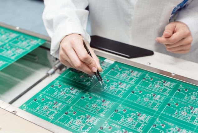
Design for Manufacturing
Design for
Testing
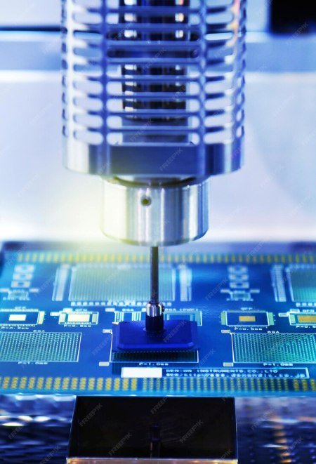
Simulation and Validation
Partner with F.Robin Technologies
Innovation demands precision, and precision is what we deliver. By choosing F.Robin Technologies, you gain a partner who understands the complexities of modern electronics and delivers solutions designed to exceed expectations. Let us empower your vision with expertly crafted PCB designs.
Let’s Innovate Together
Connect with our experts today and discover how F.Robin Technologies can accelerate your journey from concept to market.
Frequently Asked Questions
PCB design and layout is the process of placing electronic components and routing electrical traces on a printed circuit board to ensure optimal signal integrity, thermal performance, and manufacturability covering schematic capture, component placement, trace routing, and design rule verification.
The PCB layout method is a structured process covering schematic capture, component placement, power and ground plane definition, signal routing, DRC, DFM review, and Gerber file generation — reducing errors and shortening time to market.
A 2-layer PCB suits simple, low-speed circuits. A 4-layer PCB adds internal ground and power planes for better EMI control. A 6-layer PCB offers additional routing and plane layers — ideal for high-speed digital, RF, and mixed-signal applications.
Yes. All PCB layouts delivered by F.Robin Technologies comply with IPC-2221, IPC-2222, RoHS, and REACH standards. We also support designs targeting CE, FCC, UL, and IEC certifications depending on the application and industry.
The cost of a 6-layer PCB design varies based on your project’s complexity and requirements. Contact us to get a free custom quote.