
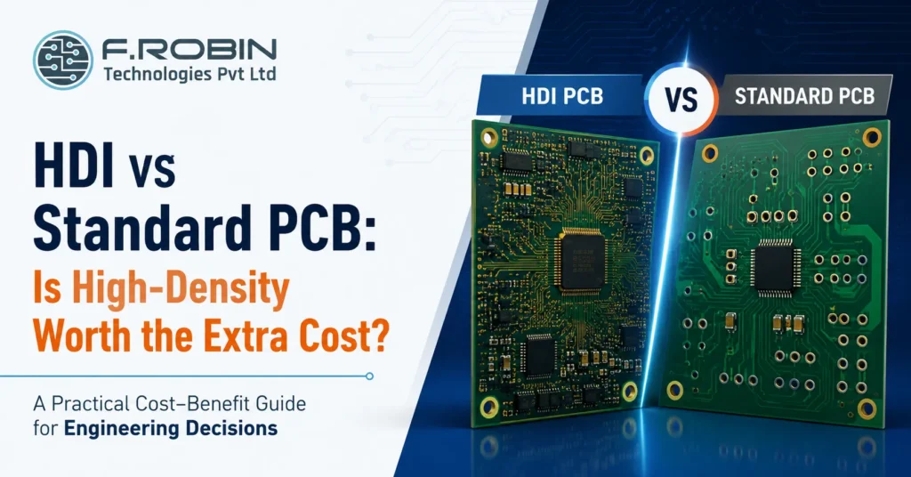
Is HDI overkill for my design?” is a fair question, because high density interconnect boards cost meaningfully more than a standard multilayer PCB and that premium is only worth paying when your design genuinely needs the density. Choosing HDI when a standard board would work wastes budget; choosing standard when HDI is truly required leads to a board that cannot be built at all.
This guide walks through the HDI vs standard PCB decision from a cost-benefit angle: what actually drives the price difference, the specific situations where HDI earns its cost, and a simple way to tell whether your design is one of them. Whether you are designing in Chennai, Bangalore, or anywhere else, the same HDI vs standard PCB evaluation applies.
The Quick Answer
In the HDI vs standard PCB decision, HDI is worth the extra cost when your design has fine-pitch BGAs that cannot be routed with a standard board, genuine space constraints, or high-speed signals that benefit from shorter via paths. It is not worth it when a standard multilayer board routes cleanly and fits your product’s size requirements.
In other words, HDI is not a premium tier you choose for its own sake it is a specific engineering solution to a specific routing or space problem. If that problem does not exist in your design, the extra cost buys you nothing.
What Drives the Cost Difference
An HDI board costs more than a standard PCB mainly because of how it is built. Standard boards are drilled and plated in a single pass; HDI boards are built up in stages, with laser-drilled microvias and, often, sequential lamination cycles that each add process time, equipment cost, and inspection.
On top of the build process, HDI boards typically demand tighter tolerances, which lowers yield and raises the effective cost per good board. Altogether, the HDI vs standard PCB cost gap commonly runs well above what a simple layer-count comparison would suggest, because the complexity is in the process, not just the material.
This is why comparing two quotes side by side rarely tells the whole story unless both are broken down by process step the headline difference in the HDI vs standard PCB quote often understates just how much of that gap comes from yield loss rather than raw material or drilling time.
When HDI Is Worth It
HDI earns its cost premium in specific, identifiable situations. A fine-pitch BGA with hundreds of closely spaced pins often cannot be escaped with standard through-hole vias at all in that case, the HDI vs standard PCB question is not really a choice, since a standard board physically cannot route the part.
Genuine size constraints are another strong justification: wearables, implantables, and compact consumer devices frequently need the routing density that only HDI delivers. High-speed designs also benefit, since shorter microvia paths reduce stub length and improve signal integrity in ways a standard board’s longer through-hole vias cannot match.
When Standard PCB Is the Better Choice
Just as often, a standard multilayer PCB is the smarter, cheaper choice. If your component pitch is generous, your layer count is modest, and the board is not fighting for space, a standard build routes just as reliably at a fraction of the cost.
This is where the “is HDI overkill” question resolves in favor of standard: reaching for HDI features a design does not structurally need adds cost and complexity without a corresponding benefit. In the HDI vs standard PCB comparison, standard wins by default whenever it can do the job HDI only wins when it must.
Side-by-Side Cost-Benefit Comparison
The table below summarizes the HDI vs standard PCB trade-off across the factors that matter most to a cost-benefit decision.
| Factor | Standard PCB | HDI PCB |
| Relative cost | Lower | Higher (often significantly) |
| Routing density | Moderate | Very high |
| Fine-pitch BGA support | Limited or none | Strong |
| Miniaturization | Limited | Enables the smallest form factors |
| Signal integrity (high speed) | Adequate for most designs | Better via shorter microvia paths |
| Best for | Generic pitch, ample space, cost-sensitive designs | Fine-pitch BGAs, tight space, high-speed designs |
Reading down the table, the pattern is consistent: HDI wins wherever density or miniaturization is the binding constraint, while standard PCB wins on cost whenever that constraint does not apply.
A Real-World Example
Picture a compact fitness tracker with a fine-pitch processor and hundreds of pins packed into a tiny footprint. Here, the HDI vs standard PCB comparison resolves quickly: a standard board simply cannot escape that many pins in that little space, so HDI is not a luxury, it is the only way to build the product at all.
Now picture an industrial control panel with a modest microcontroller, generous board area, and no unusual space constraints. The HDI vs standard PCB comparison resolves just as clearly here, but in the opposite direction a standard multilayer board routes the design comfortably, and HDI would only add cost without solving a problem that exists.
Most designs fall somewhere between these extremes, which is exactly why running the simple test below, rather than guessing, produces a more reliable answer.
A Simple Test: Is HDI Overkill for You?
- Can your fine-pitch components be escaped using standard through-hole vias? If yes, HDI may be unnecessary.
- Does your product have hard size or weight constraints that a standard board’s layer count cannot meet? If yes, HDI is likely justified.
- Are your highest-speed signals sensitive enough that via stub length is a real concern? If yes, HDI’s shorter microvias may be worth it.
- Would a standard multilayer board route cleanly with reasonable layer count? If yes, that is usually the more cost-effective answer.
If you answer “standard would work” to most of these, HDI is probably overkill for your design. If you answer “no” to the routing and space questions, HDI is likely the only real option.
Common Mistakes to Avoid
- Choosing HDI by default because it sounds more advanced, without a routing or space problem that requires it.
- Choosing standard PCB to save cost on a design with fine-pitch BGAs that genuinely cannot be routed otherwise.
- Assuming the HDI cost premium is small, when it can be substantial once sequential lamination is required.
- Deciding on stack-up before confirming actual component footprints and pitch requirements.
- Skipping a conversation with your fabricator about whether a standard board can realistically meet your routing needs.
Avoiding these keeps the HDI vs standard PCB decision grounded in your design’s real requirements rather than assumption or habit.
Key Takeaways
- HDI costs more than a standard PCB mainly due to sequential lamination, laser drilling, and tighter tolerances.
- HDI is worth it for fine-pitch BGAs, genuine space constraints, and high-speed designs sensitive to via stub length.
- Standard PCB is the better choice whenever it can route cleanly HDI should be a solution to a specific problem, not a default.
- Use the simple test component pitch, size constraints, signal speed, routing feasibility to check if HDI is overkill for your design.
- The HDI vs standard PCB cost gap is often larger than a simple layer-count comparison would suggest.
- Confirm actual routing feasibility with your fabricator before committing to either stack-up.
