
Do I really need 4 layers, or is 2 enough?” is one of the most common stack-up decisions in PCB design, and getting it wrong in either direction costs you. Choose 2 layers when the design needs 4, and you fight signal integrity and EMI problems for the rest of the project. Choose 4 layers when 2 would have worked, and you pay more per board for no real benefit.
This guide gives you a practical way to make the 2-layer vs 4-layer PCB decision covering cost, routing density, EMI, and signal integrity — so you can match the stack-up to your actual design rather than guessing or defaulting to whichever you used last time. Whether you are designing in Chennai, Bangalore, or anywhere else, the same engineering logic applies to every 2-layer vs 4-layer PCB decision you face.
The Quick Answer
In short: a 2-layer PCB is enough for simple, low-speed, low-density designs where cost matters most. A 4-layer PCB is worth the extra cost when you have a dedicated ground plane need, higher routing density, faster signals, or EMI requirements that 2 layers cannot reliably meet.
The 2-layer vs 4-layer PCB decision is not about which is generally “better” it is about matching the stack-up to what your specific circuit actually demands. Every 2-layer vs 4-layer PCB decision should start from your design’s actual requirements, not a default habit. The sections below walk through exactly how to make that call.
What a 2-Layer Board Gives You
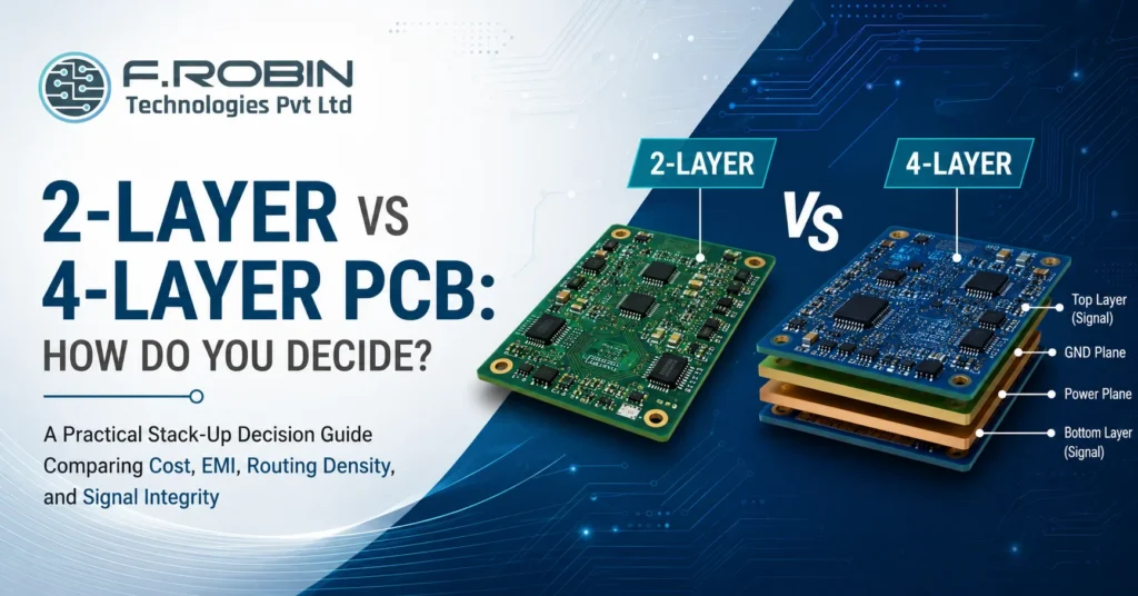
A 2-layer PCB has copper on the top and bottom only, with all routing and, typically, a partial ground plane shared across those two layers. It is the simplest, cheapest stack-up, and for many designs it is entirely sufficient.
A 2-layer board works well for simple analog or low-speed digital circuits, low pin-count microcontroller designs, power circuits without demanding EMI targets, and any design where routing is not congested. If your circuit fits comfortably with room to spare, a 2-layer PCB is usually the right, cost-effective choice.
What a 4-Layer Board Gives You
A 4-layer PCB adds two internal layers, most commonly used as a dedicated ground plane and a dedicated power plane, sandwiched between the outer signal layers. This structure gives every signal a close, continuous return path, which is the single biggest driver of better signal integrity and EMI performance.
A 4-layer board earns its cost when you have higher-speed signals, denser routing than a 2-layer board can comfortably handle, stricter EMI or EMC requirements, or a design where controlled impedance matters. The extra layers are not just about fitting more traces — they fundamentally change how clean your signals and your radiated emissions are.
Cost Comparison
A 4-layer PCB costs more than a 2-layer board typically somewhere in the range of 1.5 to 2.5 times the fabrication cost, depending on your fabricator, volume, and specifications. At low volume or for a simple design, that difference is real money for no functional benefit if 2 layers would have worked just as well.
At the same time, choosing 2 layers for a design that genuinely needs 4 often costs more in the long run: EMI failures during compliance testing, signal integrity debugging, or a board respin all cost far more than the layer-count premium would have. The right lens for the 2-layer vs 4-layer PCB decision is not “which is cheaper per board” but “which is cheaper once you include the risk of getting it wrong.”
Routing Density and Complexity
Routing density is often the most practical driver of the 2-layer vs 4-layer PCB decision. If a 2-layer layout leaves you fighting for space, adding trace-length workarounds, or routing signals through awkward paths just to avoid crossing, that struggle is a strong signal that a 4-layer board would save real engineering time.
As a rough guide, a 2-layer board comfortably handles simple designs with modest component counts and generous spacing. Once you are working with fine-pitch parts, higher pin-count ICs, or a board that feels cramped no matter how you arrange it, that congestion is usually the clearest practical signal in the whole 2-layer vs 4-layer PCB decision, and 4 layers resolves it far more cleanly than forcing a 2-layer solution.
EMI and Signal Integrity
This is where the 2-layer vs 4-layer PCB decision matters most for reliability. A dedicated ground plane in a 4-layer board gives every signal a short, low-impedance return path directly beneath it, which dramatically reduces loop area and, with it, radiated emissions.
On a 2-layer board, return paths are harder to control, especially as signal speed increases. For low-speed, simple circuits this rarely matters. For anything with faster edges, sensitive analog sections, or strict EMC compliance targets, the lack of a clean ground plane on a 2-layer board becomes a real risk one that often only surfaces during compliance testing, when it is expensive to fix.
Side-by-Side Comparison
The table below summarizes the 2-layer vs 4-layer PCB trade-off across the factors that matter most.
| Factor | 2-layer PCB | 4-layer PCB |
| Relative cost | Lowest | 1.5–2.5x higher |
| Routing density | Limited | Significantly higher |
| EMI performance | Weaker, no dedicated plane | Strong, dedicated ground plane |
| Signal integrity | Adequate for low speed | Much better for higher speed |
| Best for | Simple, low-speed, cost-sensitive designs | Dense, higher-speed, EMI-sensitive designs |
Reading down the table, the pattern is clear: 2 layers wins on cost and simplicity, while 4 layers wins wherever density, speed, or EMI performance genuinely matter.
A Real-World Example
Picture two boards. The first is a simple temperature sensor module: a handful of passives, one low-pin-count microcontroller, and a UART interface. Routing is easy, speeds are low, and there is no EMC certification requirement. This is a textbook 2-layer vs 4-layer PCB decision that resolves quickly in favor of 2 layers the extra cost of 4 layers would buy nothing this design actually needs.
The second board is a compact IoT gateway with a high-pin-count processor, USB and Ethernet interfaces, and a formal EMC certification requirement ahead of shipping. Here, the 2-layer vs 4-layer PCB decision resolves just as clearly in the other direction: routing density alone would strain a 2-layer layout, and the EMC target makes the dedicated ground plane of a 4-layer board close to essential.
Most real designs sit somewhere between these two extremes, which is exactly why running through the decision framework below rather than defaulting to instinct produces a more reliable answer than either example alone.
A Decision Framework
- Estimate routing density. Does the design fit comfortably on 2 layers, or is it a constant struggle?
- Check signal speed. Are there fast edges, high-speed interfaces, or sensitive analog sections?
- Confirm EMI/EMC requirements. Does the product need to pass formal compliance testing?
- Weigh volume against risk. At high volume, does the 4-layer premium outweigh the cost of a possible respin?
- When in doubt, favor 4 layers for anything that will ship as a certified product, and reserve 2 layers for genuinely simple, low-risk designs.
Running through this framework before finalizing your stack-up turns the 2-layer vs 4-layer PCB decision from a guess into an evidence-based one.
Common Mistakes to Avoid
- Defaulting to whichever layer count was used on the last project, without reassessing the actual design.
- Choosing 2 layers to save cost on a design with real EMI or high-speed requirements.
- Choosing 4 layers by default for a genuinely simple, low-speed design that did not need it.
- Ignoring routing congestion warnings during layout that suggest the design has outgrown 2 layers.
- Skipping EMI/EMC consideration until compliance testing, when a stack-up change is expensive to make.
Avoiding these keeps the 2-layer vs 4-layer PCB decision grounded in your design’s real needs, not habit or guesswork.
Key Takeaways
- A 2-layer PCB suits simple, low-speed, cost-sensitive designs with comfortable routing.
- A 4-layer PCB suits denser, higher-speed, or EMI-sensitive designs, thanks to its dedicated ground plane.
- 4-layer boards typically cost 1.5–2.5x more to fabricate, but can be cheaper overall once respin and compliance risk are considered.
- Routing congestion and EMI/EMC requirements are the two strongest signals that a design has outgrown 2 layers.
- Use a decision framework density, speed, compliance, volume rather than defaulting to habit for every 2-layer vs 4-layer PCB decision.
- When a design will ship as a certified product, 4 layers is usually the safer default.
