
PCB mechanical integration is the practice of designing your board and its enclosure as one system, so they fit together perfectly the first time. When it goes well, connectors line up, components clear the lid, and assembly is effortless. When it goes wrong, you get fit clashes misaligned ports, components hitting the housing, mounting holes that miss and each one can trigger an expensive board or tooling respin.
This guide explains how to get PCB mechanical integration right. We cover why fit clashes are so costly, what causes them, and the best practices that keep your board-to-enclosure design clash-free. Whether you build rugged industrial units or compact consumer devices, these techniques will save you time, money, and frustration.
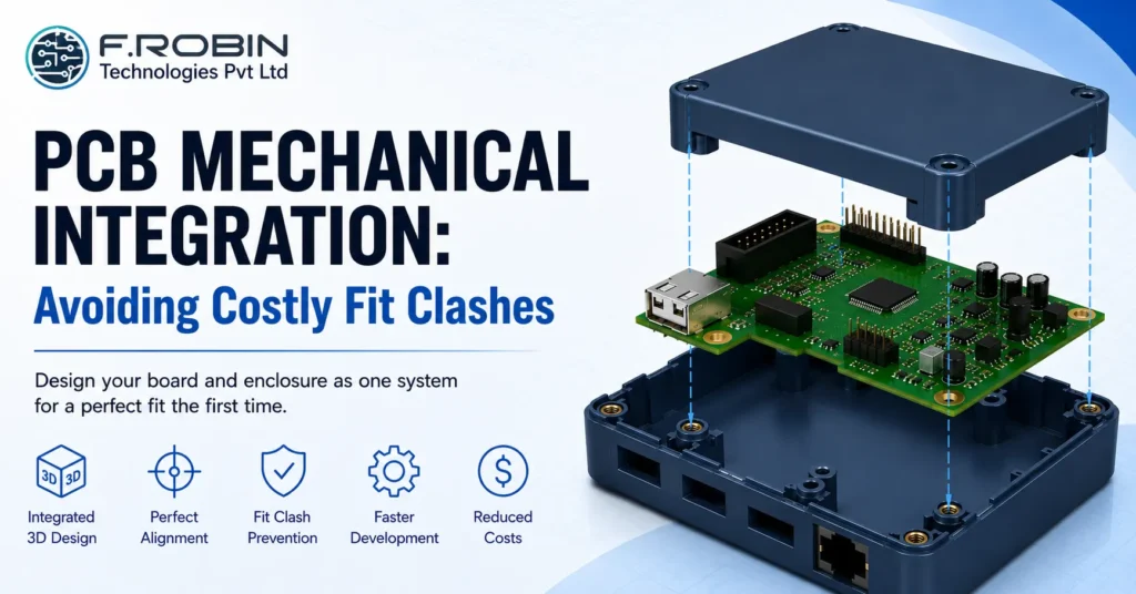
What Is PCB Mechanical Integration?
PCB mechanical integration is the coordinated design of a printed circuit board and its mechanical enclosure so the two fit and function together. It ensures the board outline, components, connectors, and mounting points all align with the housing that surrounds them.
In practice, this means the electrical and mechanical teams share information and a common 3D model throughout design. The board defines connector positions and component heights; the enclosure defines walls, cut-outs, and standoffs. PCB mechanical integration brings these two views together so nothing collides.
Done well, it is invisible — everything simply fits. Done poorly, it surfaces as clashes late in development, when fixes are most expensive. That is why treating board-to-enclosure design as one integrated task, not two separate ones, is the foundation of reliable hardware.
Why Fit Clashes Are So Costly
A single fit clash can be far more expensive than it first appears. Because mechanical and electrical issues often surface only after prototypes or tooling exist, fixing them means redoing expensive work.
Poor PCB mechanical integration leads to costly outcomes:
- Board respins when connectors or mounting holes must move.
- Tooling rework when the enclosure mould needs changes.
- Schedule slips as teams loop back through design and prototyping.
- Assembly problems when parts do not fit on the line.
- Field failures from stressed boards or poor sealing.
Each of these costs time and money that early integration would have prevented. In short, the few hours spent coordinating board and enclosure up front save weeks of rework later which is exactly why PCB mechanical integration deserves attention from day one.
Common Causes of Fit Clashes
Most fit problems trace back to a handful of recurring causes. Recognizing them early is half the battle.
- Connector misalignment. Ports that do not line up with enclosure cut-outs.
- Tall components. Capacitors or heatsinks that hit the lid or walls.
- Mounting mismatch. Standoffs and holes that do not match the board.
- Insufficient clearance. Too little space between the board and housing.
- Board outline errors. A PCB shape that does not match the enclosure cavity.
- Tolerance stack-up. Accumulated variation that pushes parts out of fit.
Almost all of these stem from designing the board and enclosure separately. When the two are integrated from the start, these clashes are caught on screen instead of on the bench.
PCB Mechanical Integration Best Practices
Follow these best practices to keep board-to-enclosure design clash-free.
- Share a common 3D model. Both teams should work from one assembly so changes are visible to everyone.
- Define the board outline and keep-out zones early. Lock the shape, edge clearances, and no-component areas before detailed work.
- Align connectors and ports first. Position connectors to match enclosure cut-outs, then design outward.
- Plan component height and clearance. Map tall components against the lid and walls to avoid collisions.
- Match mounting holes and standoffs. Ensure hole positions, diameters, and standoff heights agree exactly.
- Account for tolerance stack-up. Add realistic clearance so manufacturing variation never causes a clash.
- Use ECAD-MCAD collaboration. Exchange board and enclosure data between PCB tools and SolidWorks regularly.
- Review the full assembly in 3D before release. A final 3D check catches clashes that 2D views hide.
Applied together, these practices turn PCB mechanical integration from a source of surprises into a predictable, repeatable process. They also tie directly into broader mechanical design services, where the enclosure and board evolve as one.
The ECAD-MCAD Workflow
The technical heart of PCB mechanical integration is exchanging data between electrical CAD (ECAD) and mechanical CAD (MCAD). The PCB tool holds the board and components; the MCAD tool — often SolidWorks — holds the enclosure. Keeping them in sync is what prevents clashes.
Teams typically share data using neutral formats:
- STEP files carry full 3D geometry of the board and components into the enclosure model.
- IDF / IDX formats exchange board outline, keep-outs, and component placements between ECAD and MCAD.
- Incremental updates let mechanical and electrical teams push changes back and forth as the design evolves.
The goal is a single, shared source of truth. When the PCB moves a connector, the enclosure team sees it immediately; when the enclosure narrows a wall, the layout team adjusts. This continuous loop is what makes mechanical engineering and analysis of the assembly accurate and clash-free.
A Pre-Release Fit Checklist
Before releasing the design, run through this quick checklist:
- ✅ Board outline matches the enclosure cavity.
- ✅ All connectors align with their cut-outs.
- ✅ Tall components clear the lid and walls.
- ✅ Mounting holes and standoffs match exactly.
- ✅ Adequate clearance everywhere, including tolerance margin.
- ✅ Full 3D assembly reviewed with no interference.
- ✅ Thermal and serviceability access confirmed.
Ticking every box before release is the simplest way to avoid a costly respin. If any item fails, fix it now not after tooling.
Common Mistakes to Avoid
Even strong teams slip up on integration. Watch for these:
- Designing board and enclosure separately, then hoping they fit.
- Skipping the 3D assembly review before release.
- Ignoring tolerance stack-up, so parts clash in production.
- Forgetting clearance for cables, fasteners, and airflow.
- Locking the enclosure before the PCB is stable, forcing rework.
- Relying on 2D drawings alone, which hide real interferences.
Avoiding these keeps your PCB mechanical integration smooth and your project on schedule.
Key Takeaways
- PCB mechanical integration designs the board and enclosure as one system to prevent fit clashes.
- Fit clashes are costly because they trigger board respins, tooling rework, and schedule slips.
- Common causes include connector misalignment, tall components, mounting mismatch, and tolerance stack-up.
- Best practices: share a 3D model, lock the board outline early, align connectors, and account for tolerance.
- The ECAD-MCAD workflow (STEP, IDF/IDX, SolidWorks) keeps board and enclosure in sync.
- Always review the full 3D assembly before release.
Conclusion
PCB mechanical integration is the difference between hardware that fits the first time and a project derailed by costly respins. By designing the board and enclosure as one system — sharing a 3D model, aligning connectors early, accounting for tolerance, and reviewing the full assembly before release — you eliminate the fit clashes that wreck schedules and budgets.
Building a Product Where the PCB and Enclosure Must Fit Perfectly?
Our mechanical engineering services and PCB layout design services handle PCB mechanical integration from concept to production. Work with our engineering team to eliminate design clashes, reduce development risk, and accelerate time to market.
Talk to Our Engineering TeamFrequently Asked Questions
1. What is PCB mechanical integration?
PCB mechanical integration is the coordinated design of a printed circuit board and its enclosure so they fit and function together, aligning the board outline, components, connectors, and mounting points with the housing.
2. Why is PCB mechanical integration important?
It prevents costly fit clashes — misaligned connectors, components hitting the lid, or mismatched mounting holes — that would otherwise trigger board respins, tooling rework, and schedule delays.
3. What causes PCB-enclosure fit clashes?
Common causes are connector misalignment, tall components, mismatched mounting holes, insufficient clearance, board outline errors, and tolerance stack-up — usually from designing board and enclosure separately.
4. What is the ECAD-MCAD workflow?
The ECAD-MCAD workflow exchanges data between electrical CAD (the PCB) and mechanical CAD (the enclosure, often in SolidWorks) using STEP and IDF/IDX formats, keeping both designs in sync.
5. How do I avoid connector alignment problems?
Align connectors and ports with enclosure cut-outs early, share a common 3D model, and include tolerance margin so manufacturing variation does not cause misalignment.
