
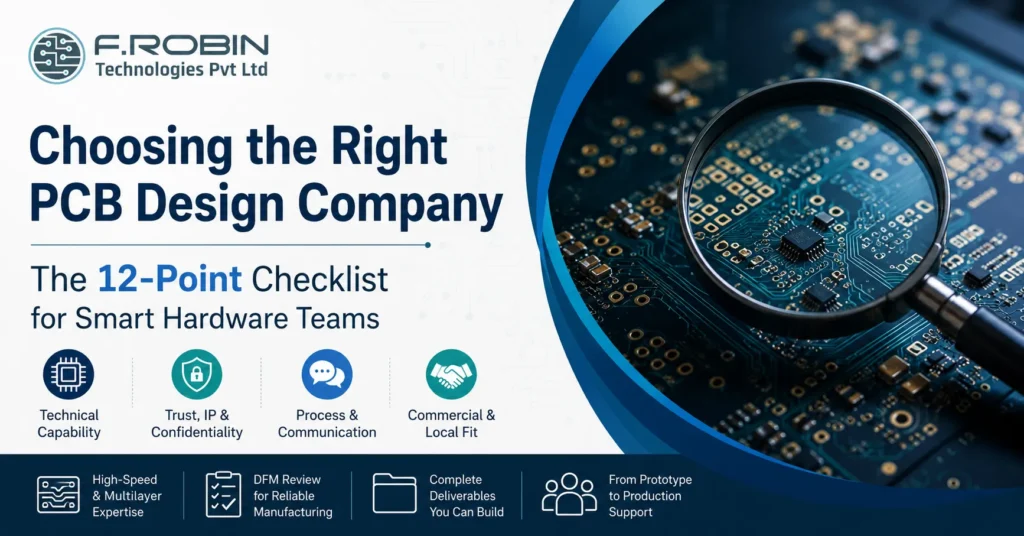
Choosing the right PCB design company can make or break your hardware project. The right partner ships clean, manufacturable boards on time; the wrong one drains your budget with respins, missed deadlines, and IP worries. So before you sign anything, you need a way to separate a capable PCB design company from a risky one.
This 12-point checklist gives you exactly that. We cover technical capability, trust and IP protection, process and communication, and commercial and local fit. Whether you are searching for a “pcb design company near me,” evaluating a PCB design firm in Chennai, or comparing offshore PCB design services, these 12 questions will help you commit with confidence.
Why Choosing the Right PCB Design Company Matters
Your PCB design company shapes the cost, reliability, and time-to-market of your entire product. Because layout errors surface only after fabrication, a weak partner can cost you weeks and lakhs in respins. A strong one, by contrast, catches problems early and hands you a board that simply works.
The stakes are highest for complex boards. High-speed, mixed-signal, and dense designs demand real expertise, not just software access. Therefore, vetting your PCB design services partner carefully is not bureaucracy it is risk management. The checklist below turns that vetting into a simple, repeatable process.
Consider the ripple effects too. A delayed board pushes back firmware, testing, certification, and launch, so a single weak link in design can slip an entire product roadmap. Conversely, a partner who gets the layout right the first time protects every downstream milestone. That is why the few hours you spend vetting a partner up front pay back many times over.
The 12-Point Checklist for Choosing a PCB Design Company
Work through these four areas. Each contains three questions to ask any candidate before you commit.
Technical Capability (Points 1–3)
- Do they have relevant domain experience? Ask for examples of boards similar to yours — same speed class, layer count, and industry. Proven PCB designers in your domain reduce risk dramatically.
- Can they handle your complexity? Confirm they routinely do high-speed, multilayer, and mixed-signal work, and that they can support signal integrity analysis when needed.
- Which tools and standards do they use? A credible PCB design firm works in professional tools and follows IPC standards for your required class.
Trust, IP & Confidentiality (Points 4–6)
- Do they offer a clear NDA? Strong IP/NDA practices protect your design files. A serious partner will sign one without hesitation.
- Is the work done by in-house design teams? Ask directly: do they use in-house design engineers, or quietly subcontract your IP to third parties? In-house teams mean better security and accountability.
- How do they handle your data and ownership? Confirm you own all deliverables and that files are stored securely throughout the project.
Process & Communication (Points 7–9)
- Do they perform a DFM review? A DFM review (design for manufacturability) before release prevents costly fabrication and assembly issues.
- How will they communicate? Clear cadence, a single point of contact, and manageable timezone overlap keep projects on track.
- What does their deliverable package include? Expect schematics, layout files, Gerber/ODB++ data, BOM, and assembly drawings not just a board file.
Commercial & Local Fit (Points 10–12)
- Is their pricing transparent? Watch for vague quotes and hidden NRE or revision fees. A trustworthy firm explains exactly what you pay for.
- Are they a good local fit? If you searched “pcb design company near me,” weigh the benefits of a local PCB design company in Chennai easier collaboration, shared timezone, and faster meetings.
- Can they scale with you? The best partner supports you from prototype through volume, often as a Make in India PCB service that keeps design and manufacturing close together.
Quick Checklist Table
Use this summary to score any candidate at a glance.
| Check | What “Good” Looks Like |
|---|---|
| 1. Domain Experience | Similar boards successfully designed in your industry |
| 2. Complexity Capability | Experience with high-speed, multilayer, and mixed-signal designs |
| 3. Tools & Standards | Professional design tools and IPC compliance |
| 4. NDA Offered | Signed without hesitation to protect intellectual property |
| 5. In-House Design | No hidden subcontracting or outsourcing |
| 6. Data & Ownership | You retain ownership of all design files and deliverables |
| 7. DFM Review | Design for Manufacturability review completed before release |
| 8. Communication | Single point of contact with clear project updates and cadence |
| 9. Deliverable Package | Complete manufacturing data package provided |
| 10. Transparent Pricing | No hidden fees or unexpected charges |
| 11. Local Fit | Convenient collaboration and time-zone alignment |
| 12. Ability to Scale | Support from prototype development through volume production |
In-House vs Outsourced PCB Design Company
Should you build a layout team or hire a PCB design company? The table below compares the options.
| Factor | In-House Team | PCB Design Company |
|---|---|---|
| Upfront Cost | High (salaries, software licenses, and hardware) | Low (project-based engagement) |
| Flexibility | Fixed capacity based on team size | Scales up or down with project demand |
| Expertise Range | Limited to the skills of your hired engineers | Broad experience across industries and project types |
| Tool Licensing | You purchase and maintain design tools | Typically included as part of the service |
| Best For | Continuous, high-volume PCB development | Variable workloads or specialized design requirements |
For most teams with variable workloads, a capable PCB design firm delivers senior expertise without the fixed overhead. Many companies blend both keeping core work in-house and outsourcing specialized or overflow projects to trusted PCB design services.
Red Flags to Watch For
Beyond the checklist, these warning signs should give you pause:
- Reluctance to sign an NDA or vague answers about IP protection.
- No portfolio or examples relevant to your board type.
- Hidden subcontracting instead of true in-house design.
- Quotes far below market a sign of inexperience or hidden costs.
- No DFM review in their process.
- Poor communication during the sales stage, which only worsens later.
If you spot several of these, keep looking. The cost of choosing the wrong partner always exceeds the cost of vetting carefully.
How to Run Your Evaluation (Step by Step)
Turn the checklist into action with a simple process:
- Shortlist three to five candidates. Mix local and remote options so you can compare fairly.
- Request a relevant portfolio. Ask each firm for boards similar to yours in speed, layer count, and industry.
- Send the same brief to all. A consistent brief makes quotes and timelines directly comparable.
- Sign NDAs early. Confirm IP/NDA terms before you share sensitive design details.
- Score each candidate against the 12-point table, then weight the factors that matter most to your project.
- Run a small paid pilot. A short trial — a sub-circuit or a single board section — reveals real communication and quality far better than a sales call.
- Decide and document. Choose the partner with the best overall score, not just the lowest price.
This structured approach removes guesswork. Moreover, a paid pilot is the single most reliable predictor of how a partner will perform on your full project.
Local vs Offshore: Weighing a Partner Near You
Location affects collaboration, cost, and IP comfort. A nearby firm say, one in Chennai or elsewhere in India offers shared working hours, easier face-to-face reviews, and quicker design iterations. Offshore options may look cheaper, yet timezone gaps and slower feedback can erode that saving on complex boards.
For many Indian OEMs and startups, a Make in India PCB service strikes the best balance: local collaboration, strong IP protection, and the option to keep design and manufacturing under one roof. Weigh proximity against capability and never trade away expertise purely to be close. If you searched for a “pcb design company near me,” use distance as a tie-breaker between strong candidates, not as the deciding factor on its own.
Key Takeaways
- Vet any PCB design company across capability, trust/IP, process, and commercial fit.
- Confirm domain experience, complexity handling, and IPC-standard tools.
- Insist on a clear NDA, in-house design, and full data ownership.
- Require a DFM review and a complete deliverable package.
- Weigh local fit ma PCB design company near you or in Chennai eases collaboration.
- Choose a partner that scales from prototype to a Make in India PCB service.
Conclusion
Choosing a PCB design company does not have to be a gamble. Run every candidate through the 12-point checklist technical capability, trust and IP protection, process and communication, and commercial and local fit and the right partner becomes obvious. Above all, insist on a clear NDA, genuine in-house design, a DFM review, and transparent pricing.
Looking for a Reliable PCB Design Partner?
If you want a partner that ticks all 12 boxes, our PCB layout design services combine in-house engineering expertise, IPC-compliant quality, and a Make in India PCB service that supports your project from prototype through volume production. Discuss your requirements with our engineering team and move your next board forward with confidence.
Talk to Our Engineering TeamFrequently Asked Questions
1. How do I choose a PCB design company?
Evaluate a candidate across four areas: technical capability, trust and IP protection, process and communication, and commercial and local fit. Use a 12-point checklist and require a signed NDA, DFM review, and a full deliverable package.
2. What should I ask a PCB design company before hiring?
Ask about domain experience, complexity capability, tools and standards, NDA and IP handling, in-house design, DFM review, communication cadence, deliverables, pricing transparency, and ability to scale.
3. Is it better to use a local PCB design company?
A local partner—for example, a firm in Chennai—offers easier collaboration, shared time zones, and faster meetings. For complex projects, that proximity can speed up reviews and reduce miscommunication.
4. How much do PCB design services cost?
Cost depends on layer count, complexity, and revisions. A reputable provider gives transparent quotes with no hidden NRE or revision fees, so always confirm exactly what is included.
5. Why does in-house design matter when choosing a PCB design firm?
In-house design means your IP stays with one accountable team rather than being subcontracted. This improves security, quality control, and communication.
