
Introduction
The types of PCB manufacturing process determine everything downstream board complexity, layer count, material choice, cost, lead time, and the electrical performance of the finished board. Yet for most hardware teams, the manufacturing process is a black box: you send Gerbers, you receive boards.
Understanding what actually happens inside that black box — and which process applies to which board type helps you make better design decisions, write more accurate specifications, choose the right fabricator, and avoid costly surprises at the DFM stage.
In this guide, we cover every major PCB manufacturing process type, what each involves, when each is appropriate, and how they compare on cost, capability, and quality.
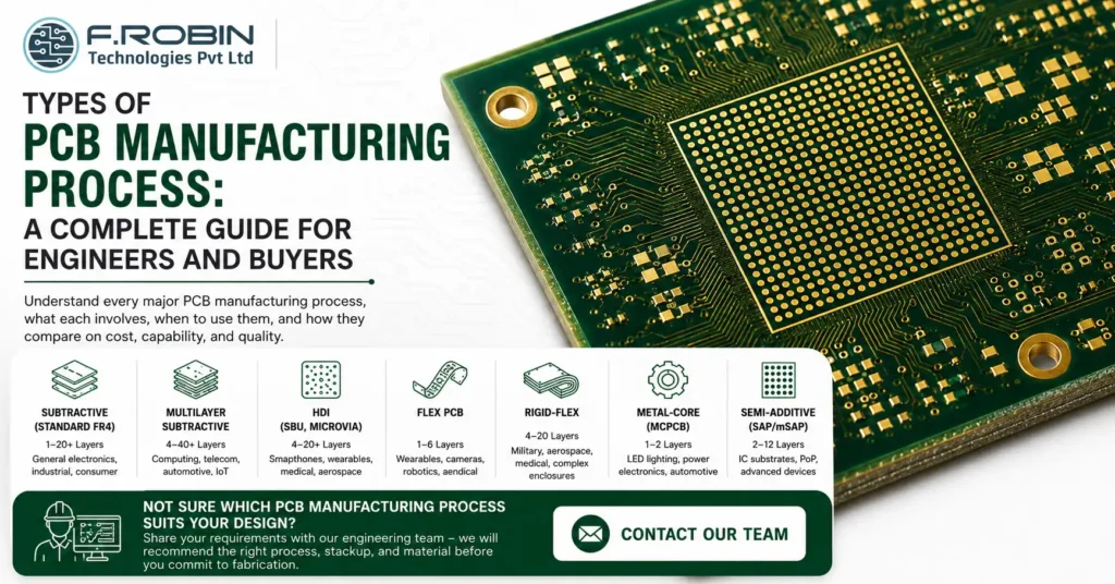
1. The Core PCB Manufacturing Process Subtractive Fabrication
The most widely used PCB manufacturing process globally is subtractive fabrication also called the subtractive method or print-and-etch process. It is the standard process for the vast majority of FR4 rigid PCBs manufactured today, from single-layer boards to complex multilayer designs.
How the subtractive process works
The subtractive process starts with a copper-clad laminate a fibreglass substrate (FR4) with copper foil bonded to one or both sides. The unwanted copper is selectively removed through a sequence of imaging, etching, and plating steps, leaving behind only the copper traces, pads, and planes defined by the design.
Preparing the Inner Layers
Step 1 — Photolithography (inner layer imaging) The copper surface is coated with a light-sensitive photoresist. A photomask or in modern facilities, a laser direct imaging (LDI) system exposes the circuit pattern onto the resist. Consequently, the unexposed resist is washed away, and the exposed copper underneath is chemically etched off. What remains is precisely the copper circuit pattern of that layer.
Step 2 — Lamination For multilayer boards, the individual inner layers are stacked with prepreg (glass-fibre epoxy resin sheets) between them and bonded under heat and pressure in a hydraulic lamination press. As a result, all layers fuse into a single rigid, uniform substrate.
Step 3 — Mechanical and laser drilling CNC drilling machines create holes for through-hole component leads, via connections between copper layers, and mechanical mounting points. In addition, high-density boards use laser drilling to create microvias holes too small for mechanical drills, typically under 150µm in diameter.
Finishing the Board
Step 4 — Through-hole plating The drilled holes are copper-plated by electroless deposition followed by electrolytic plating, creating a conductive copper barrel through the hole that electrically connects layers. This step is fundamentally what distinguishes a multilayer PCB from a simple stack of copper sheets.
Step 5 — Outer layer imaging and etching Following plating, the outer copper layers go through the same photolithography and etching process as the inner layers, defining the surface traces, pads, and planes.
Step 6 — Solder mask, surface finish, and silkscreen A liquid photoimageable solder mask (LPI) is applied and cured, opening only the pad areas. A surface finish (HASL, ENIG, OSP, or hard gold) is applied to exposed pads. Finally, reference designators and component outlines are printed as silkscreen.
Step 7 — Electrical test and delivery Every board is electrically tested by flying probe or bed of nails before shipment, verifying continuity and absence of shorts.
The subtractive process is cost-effective, mature, and supported by every PCB fabricator in India and globally. For standard FR4 rigid boards — single layer through to 20+ layers it remains the default manufacturing method.
2. Multilayer PCB Manufacturing Process
Multilayer PCB manufacturing follows the same subtractive process as single and double-sided boards, but adds repeated lamination cycles to build up the layer stack. It is the dominant process for all complex, high-density electronic designs.
What makes multilayer manufacturing different
Layer count options Multilayer boards are built in even numbers of layers: 4, 6, 8, 10, 12, and up to 40+ layers for advanced computing and telecommunications hardware. Each additional pair of layers adds one lamination cycle, drilling pass, and plating step.
Inner Layer Processing
Core fabrication Each inner layer starts as a separate copper-clad core a rigid substrate with copper on both sides. The circuit pattern is imaged and etched onto each core individually before the stack is assembled. Crucially, inner layers cannot be reworked after lamination, so imaging yield at this stage must be near-perfect.
Prepreg and stackup Between each core, sheets of prepreg (B-stage epoxy glass) are placed. The stackup sequence which layers are signal, power, or ground is defined by the designer and must be communicated to the fabricator in the stackup specification. Signal integrity, controlled impedance, and EMI performance all depend on correct stackup execution.
Via Types in Multilayer Boards
Through-hole vias pass from the top surface to the bottom surface through all layers. They are drilled after lamination and plated in a single pass the most common and least expensive via type.
Blind vias connect an outer layer to one or more inner layers without passing all the way through the board. They require sequential lamination laminating a partial stack, drilling and plating, then laminating further layers on top.
Buried vias connect two or more inner layers without reaching either outer surface. They are drilled and plated before lamination and are invisible in the finished board.
Microvias are laser-drilled vias with diameters typically below 150µm, used in HDI (High-Density Interconnect) designs. They enable very high component density by connecting adjacent layers over a very short distance.
Multilayer PCB manufacturing requires tighter process control than single or double-sided boards because registration errors between layers compound with each added layer. For a 12-layer board, the inner layer alignment tolerance must be held across 10 separate imaging and etching cycles.
3. HDI PCB Manufacturing Process (High-Density Interconnect)
HDI PCB manufacturing is a specialised extension of multilayer fabrication designed for boards with extremely high component density smartphones, wearables, advanced IoT modules, medical implants, and aerospace electronics.
What defines HDI manufacturing
HDI boards are characterised by line widths and spaces below 100µm, via diameters below 150µm (microvias), via-in-pad structures, and sequential build-up (SBU) lamination. As a result, they achieve far greater routing density than standard multilayer boards of the same layer count.
Sequential Build-Up (SBU) Process
Layer 1 build-up A core multilayer board is first fabricated using the standard subtractive process. Laser-drilled microvias are then created in the outer copper layers, plated, and filled. A new dielectric layer is laminated on top, and the process repeats.
Multiple build-up cycles Each SBU cycle adds a new pair of layers with their own microvias. Common HDI structures include 1+N+1 (one build-up layer each side), 2+N+2, and any-layer HDI (every layer interconnected by microvias). Each additional build-up cycle increases cost significantly.
Via-in-Pad Design
In HDI boards, microvias are often placed directly on component pads a technique called via-in-pad or VIPPO (Via-In-Pad Plated Over). This requires the microvia to be copper-filled and planarised (ground flat) so the pad surface is flat enough for solder paste and component placement. Consequently, HDI manufacturing requires additional copper fill and planarisation steps not present in standard multilayer fabrication.
HDI PCB manufacturing is available in India but is restricted to a smaller number of well-equipped fabricators. When specifying HDI, always confirm the fabricator’s minimum via diameter, SBU capability, and copper fill process before submitting files.
4. Flexible and Rigid-Flex PCB Manufacturing Process
Flexible PCB (flex PCB) manufacturing uses polyimide (PI) film as the substrate instead of rigid FR4, producing boards that can bend, fold, or conform to curved surfaces. Rigid-flex PCBs combine rigid FR4 sections with flexible polyimide sections in a single integrated assembly.
Flex PCB manufacturing
Substrate preparation Polyimide film typically Kapton is bonded with adhesiveless or adhesive-based copper foil. The subtractive etching process is then applied in the same way as rigid PCBs, but with tooling adapted for the flexible substrate.
Coverlay application Instead of solder mask, flex PCBs use a polyimide coverlay a flexible film with adhesive laminated over the circuit. Openings for pads are pre-punched in the coverlay before lamination. This step replaces the photoimageable solder mask used on rigid boards.
Stiffener attachment In areas where components are soldered (connector pads, IC landing areas), FR4 or polyimide stiffeners are adhesive-bonded to the back of the flex to provide mechanical support during assembly and use.
Rigid-flex PCB manufacturing
Rigid-flex boards are significantly more complex to fabricate than either rigid or flex boards alone. The rigid sections are built as multilayer cores; the flex sections are built as continuous flex layers that run through the entire board. Both are then laminated together in a single controlled process.
Key considerations for rigid-flex Bend radius must be specified by the designer the minimum bend radius for a given flex stack-up determines whether the board will survive its required flex cycles without cracking copper traces. Furthermore, the transition zones between rigid and flex sections require specific coverlay and stiffener geometry to prevent stress concentration.
Rigid-flex PCBs are commonly used in medical devices, military electronics, aerospace wiring harnesses, and any application where the PCB must conform to a three-dimensional geometry inside an enclosure.
5. Metal-Core PCB Manufacturing Process (MCPCB)
Metal-core PCBs replace the fibreglass core of standard FR4 with an aluminium, copper, or steel base layer. The primary purpose is thermal management the metal core conducts heat away from components far more efficiently than FR4.
MCPCB layer structure
A typical single-layer MCPCB consists of three layers:
- Metal base — aluminium (most common), copper, or steel
- Dielectric layer — a thermally conductive but electrically insulating polymer bonded to the metal base
- Copper circuit layer — the circuit is etched onto the top copper layer in the standard subtractive process
Thermal performance
The dielectric layer’s thermal conductivity measured in W/m·K is the critical performance parameter. Standard FR4 has a thermal conductivity of approximately 0.3 W/m·K. In contrast, MCPCB dielectric layers range from 1.0 to 4.0 W/m·K, and the aluminium base itself conducts at 160–205 W/m·K. As a result, MCPCBs are used wherever component junction temperatures must be kept low LED lighting, power converters, motor drives, and automotive electronics.
Manufacturing considerations
MCPCB fabrication requires adapted drilling and routing equipment because the metal base is much harder than FR4. Standard carbide drill bits wear out faster, and routing requires diamond-coated or solid carbide tooling. Additionally, the chemical compatibility of the dielectric layer with standard etchants must be verified before processing.
6. Additive and Semi-Additive PCB Manufacturing Processes
While subtractive etching is the dominant process, additive and semi-additive methods are gaining traction for ultra-fine-line designs and certain specialised applications.
Fully additive process
In a fully additive process, copper is deposited only where it is needed on the circuit pattern rather than starting with a full copper layer and etching away the unwanted portions. Copper is selectively deposited by electroless plating through a plating resist mask. As a result, there is no copper waste, and extremely fine lines (below 25µm) can be achieved without the undercut issues that limit subtractive etching.
Semi-additive process (SAP and mSAP)
The semi-additive process (SAP) starts with an ultra-thin copper seed layer on the substrate. A plating resist is then applied and patterned, and additional copper is electroplated only in the circuit areas. The resist is stripped, and the thin seed layer is flash-etched away. Because only a very thin copper layer is etched (rather than a full 18µm or 35µm foil), trace definition is much sharper and line widths below 30µm are achievable.
Modified semi-additive process (mSAP) is used by leading smartphone and high-performance computing PCB manufacturers for package substrates and the most advanced HDI boards. Notably, it is the process behind the substrate layers in flagship mobile processors.
Additive and semi-additive processes are not yet widely available from standard Indian PCB fabricators but are relevant for teams designing advanced IC substrates, ultra-miniaturised IoT modules, or package-on-package (PoP) designs.
7. Comparing PCB Manufacturing Process Types
Here is a summary comparison across all major process types to guide specification and supplier selection:
| Process Type | Layer Count | Min Line/Space | Key Application | Relative Cost |
|---|---|---|---|---|
| Subtractive (Standard FR4) | 1–20+ | 100µm / 100µm | General electronics, industrial, consumer | Low–Medium |
| Multilayer Subtractive | 4–40+ | 75µm / 75µm | Computing, telecom, automotive, IoT | Medium |
| HDI (SBU, Microvia) | 4–20+ | 50µm / 50µm | Smartphones, wearables, medical, aerospace | High |
| Flex PCB | 1–6 | 75µm / 75µm | Wearables, cameras, robotics, medical | Medium–High |
| Rigid-Flex | 4–20 | 75µm / 75µm | Military, aerospace, medical, complex enclosures | High–Very High |
| Metal-Core (MCPCB) | 1–2 | 100µm / 100µm | LED lighting, power electronics, automotive | Medium |
| Semi-Additive (SAP/mSAP) | 2–12 | 15–30µm | IC substrates, PoP, advanced mobile devices | Very High |
8. Which PCB Manufacturing Process Is Right for Your Design?
Choosing the correct process type starts with four questions:
1. What are your electrical requirements? High-speed digital, RF, or controlled impedance designs need multilayer or HDI to manage signal integrity. Standard digital and analogue circuits work well on 2–4 layer subtractive boards.
2. What are your thermal requirements? If your design dissipates more than 1W per component or uses high-power LEDs, consider MCPCB. For standard SMD power management, a well-designed 4-layer FR4 board with thermal vias is usually sufficient.
3. What are your form factor requirements? If the board must bend, fold, or fit a non-planar enclosure, flex or rigid-flex is required. For all other applications, rigid FR4 is preferred for its lower cost and wider supplier availability.
4. What is your volume and budget? HDI and rigid-flex carry significant cost premiums that are justified at volume but expensive for prototypes. For early-stage development, design on standard multilayer FR4 and migrate to HDI or rigid-flex only when the form factor or density genuinely requires it.
For detailed guidance on which PCB manufacturing process suits your specific project, F.Robin Technologies’ engineering team provides free DFM consultation and stackup recommendations before you commit to fabrication. Visit frobintech.com/pcb-manufacturing to learn more about our full manufacturing capability.
Conclusion
Understanding the types of PCB manufacturing process is not just useful knowledge for engineers it is a practical tool for making better design decisions, writing accurate fabrication specifications, evaluating supplier capability, and controlling cost across the product development lifecycle.
Whether your project calls for standard subtractive FR4, high-density HDI, thermally efficient metal-core, or mechanically flexible rigid-flex, the manufacturing process shapes every aspect of your board’s performance, cost, and lead time.
Choosing a manufacturing partner who understands all of these process types and can advise on the right one for your application is as important as choosing the right process itself.
F.Robin Technologies provides PCB fabrication and assembly services across all major board types multilayer, HDI, rigid-flex, flex, and metal-core manufactured and assembled to IPC, ISO, and UL standards from our facility.
Not Sure Which PCB Manufacturing Process Suits Your Design?
Share your requirements with our engineering team — we will recommend the right process, stackup, and material before you commit to fabrication.
Contact Our Team