

Power integrity analysis is the step most PCB design teams skip — until a board fails in the field and no one can explain why.
The symptoms are familiar: random resets, corrupted data, thermal hotspots, intermittent logic errors. Nine times out of ten, the root cause isn’t the schematic. It’s the power delivery network quietly failing to deliver clean, stable voltage to the components that depend on it.
Modern ICs operate on rails as low as 0.8 V with tolerances tighter than ±3%. A 30 mV voltage drop that would have been irrelevant on legacy 5 V hardware is now the difference between a functioning system and a field return. PI analysis finds these problems during layout — when fixing them costs engineering hours, not full board respins.
This guide covers what power integrity analysis is, what it catches, and how it protects your PCB’s reliability from design through production.
What Is Power Integrity Analysis?
Power integrity analysis is the simulation-based process of validating that every component on a PCB receives clean, stable voltage within its specified tolerance — under all operating conditions.
It evaluates three distinct but related phenomena:
- DC voltage drop (IR drop): Resistive losses in copper traces and planes that reduce voltage at the load
- AC PDN impedance: The frequency-dependent impedance of the power distribution network that governs how the board responds to switching transients
- Voltage ripple and noise: High-frequency fluctuations on power rails caused by switching regulators, simultaneous switching outputs, and load transients
PI analysis uses EDA tools — Ansys SIwave, Cadence PowerDC, Siemens HyperLynx PI — to model your actual PCB geometry, stackup, via structures, and decoupling capacitor placement. The result is a quantitative prediction of your power delivery performance before a single board is manufactured.
Why PCB Power Integrity Failures Are Hard to Diagnose
Power integrity failures are particularly damaging because they mimic other failure modes. An engineer chasing a firmware bug or a signal integrity issue may spend weeks before tracing the root cause to a collapsing power rail.
Here’s why they’re difficult to catch without PI analysis:
They’re load-dependent. A rail may measure correctly at idle but sag below minimum voltage under peak current load — the exact condition during functional testing or in-field operation.
They’re frequency-dependent. PDN resonance only becomes destructive at specific switching frequencies. A board may pass bench validation at room temperature only to fail after thermal soak shifts component behavior.
They’re intermittent. Voltage sag during a DDR memory burst or FPGA fabric switching event lasts nanoseconds. Standard bench probing misses it entirely without a high-bandwidth power rail probe and deliberate triggering.
Running power integrity analysis during layout eliminates the guesswork. Instead of diagnosing failures on physical hardware, engineers identify and fix them in simulation — where the iteration cost is near zero.
What PI Analysis Catches: The Four Critical Failure Modes
1. IR Drop — Voltage Starvation at the Load
IR drop occurs when DC current flows through copper traces and planes with finite resistance. The voltage at the load is always lower than the source voltage, and in high-current designs that difference can be significant.
A 2 A load drawing current through a narrow trace with 15 mΩ of resistance loses 30 mV — a 3.75% drop on a 0.8 V rail that immediately puts the IC outside its specified operating window. IR drop analysis produces color-coded voltage maps across your entire copper geometry, identifying exactly which paths exceed your voltage budget.
2. PDN Resonance — Noise Amplification at Specific Frequencies
Every power distribution network has resonant frequencies governed by its inductance and capacitance. At resonance, PDN impedance spikes. Any switching energy injected at that frequency — from a voltage regulator, FPGA switching fabric, or DDR memory bus — gets amplified rather than absorbed.
PDN resonance often explains why a design passes bench testing but fails EMI compliance. The noise is there; it’s just waiting for the right operating condition to become destructive.
3. Insufficient or Misplaced Decoupling — Capacitors That Don’t Contribute
Decoupling capacitors suppress transient voltage drops by providing local charge. But their effectiveness depends on placement, value, and package size. A 100 nF capacitor placed 15 mm from an IC power pin has more inductance in its connection path than capacitance in its operating range. It contributes almost nothing to PDN impedance at the frequencies that matter.
PI analysis shows which capacitors are actively reducing impedance and which are dead weight. This allows engineers to eliminate unnecessary components and reposition effective ones — reducing BOM cost while improving power integrity.
4. Voltage Ripple — Rail Noise That Corrupts Sensitive Circuits
Voltage ripple is the AC noise riding on top of a nominally stable DC supply. Its sources include switching regulator output ripple (at the converter’s switching frequency and harmonics), simultaneous switching outputs (SSO) from high-density I/O banks, and load current transients during memory bursts or processor state changes.
For most digital logic, moderate ripple is tolerable. For ADCs, PLLs, RF front ends, and high-speed SerDes interfaces, it is not. Even millivolt-level noise on a PLL supply rail introduces phase jitter. Millivolt noise on an ADC reference rail degrades SNR in ways that look like a firmware calibration problem until the power rail is measured with sufficient bandwidth.
How IR Drop Analysis Works
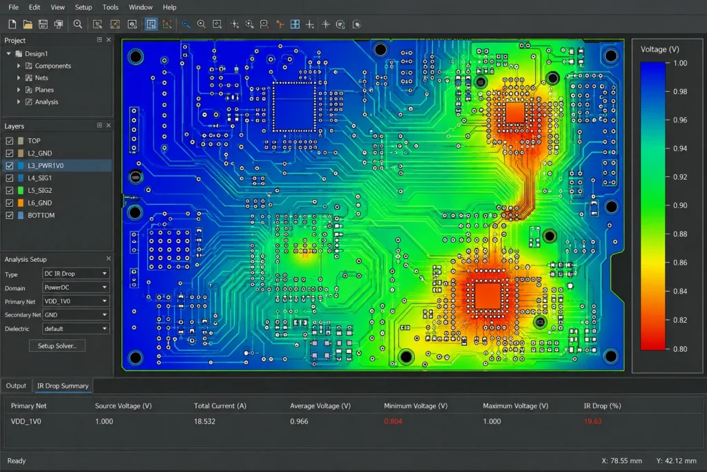
IR drop analysis is the DC simulation component of power integrity analysis. The workflow:
- Import PCB layout into a PI simulation tool
- Define current sources and sinks — power entry points and each component’s current draw at typical and peak load conditions
- Set copper material properties — conductivity, plane thickness, via geometry
- Run DC simulation — the solver computes current density and voltage distribution across all copper structures
- Review voltage maps — heat maps show where voltage at the load falls outside tolerance
- Iterate — widen traces, add via arrays, adjust plane geometry, re-run until all violations are cleared
A properly executed IR drop analysis catches the difference between a 0.9 V rail delivering 0.9 V at the source and 0.83 V at the IC power pin — a 7.7% deviation that guarantees intermittent failure under load.
PDN Analysis and Target Impedance Explained
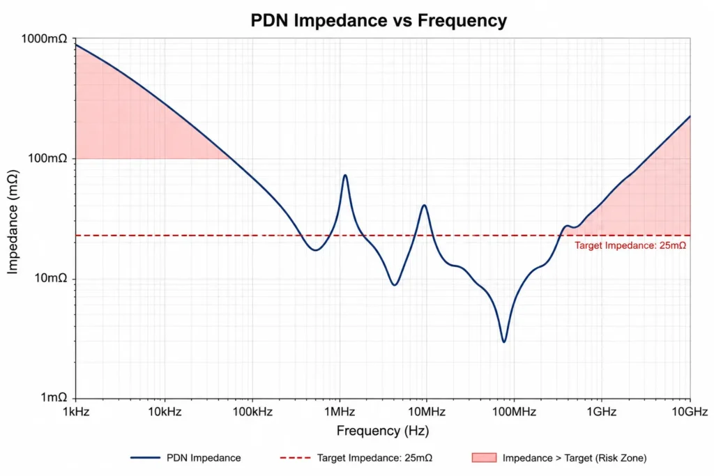
PDN analysis extends power integrity into the frequency domain. The goal is to keep the PDN impedance below a calculated target value — the target impedance — across the full frequency range where your devices switch.
Target impedance formula:
Z_target = ΔV ÷ ΔI
Where ΔV is your acceptable voltage ripple (typically 5% of rail voltage) and ΔI is the peak transient current demand.
Worked example: A 1.0 V rail with a 5% ripple budget and a 2 A transient load → Z_target = 0.05 ÷ 2 = 25 mΩ
PDN analysis plots your actual impedance vs. frequency and overlays the target line. Any frequency range where your PDN exceeds the target is a risk zone that requires design intervention — typically through:
- Bulk capacitors for low-frequency compliance (10 µF–1000 µF)
- Ceramic MLCCs close to IC power pins for mid-frequency compliance (100 nF–10 µF)
- Adjacent power/ground planes for high-frequency, distributed capacitance
- Embedded capacitance laminates for ultra-high-frequency designs
Voltage Ripple Analysis: Protecting Sensitive Circuits
Voltage ripple analysis combines time-domain and frequency-domain simulation to evaluate AC noise on power rails. In practice, it answers three questions:
- Which switching events produce the largest voltage deviation on each rail?
- How far does that noise propagate through the PDN before it is attenuated?
- Does the decoupling strategy suppress ripple at the IC power pin to within acceptable limits?
For designs with mixed analog-digital supply domains, this analysis also maps how noise from a switching digital rail couples into an adjacent analog supply through shared planes or poorly isolated return paths — one of the most common causes of ADC performance degradation that evades standard signal integrity analysis.
How to Achieve Power Integrity in Your PCB Design
- Design Your Stackup With Adjacent Power and Ground Planes
Place power and ground planes on neighboring layers with thin dielectric between them. This creates natural inter-plane capacitance that reduces high-frequency PDN inductance across the entire board.
- Size Copper Geometry for Actual Load Current
Use IPC-2221 tables to size every high-current trace based on real component current draw — not default pour widths. Check plane splits and cutouts for hidden resistance chokepoints before routing begins.
- Apply a Three-Tier Decoupling Strategy
Use bulk capacitors at the regulator output, mid-frequency ceramics at each IC power entry, and high-frequency MLCCs at every IC power pin. Each tier targets a different frequency band — no single value covers the full switching range.
- Place Decoupling Capacitors Within 2–3 mm of IC Power Pins
Keep every decoupling capacitor as close as physically possible to the IC power pin it serves. Long routing traces add parasitic inductance that reduces the capacitor’s effectiveness at high frequencies.
- Use Multiple Parallel Vias on Every Power Connection
Replace single vias with arrays of two or more on all power connections. Parallel vias reduce inductance and share current load — critical at BGA power balls, regulator outputs, and PDN entry points.
- Keep High-Speed Routes Away From Plane Splits
Never route DDR, SerDes, clock, or FPGA signals across a plane split. Splits force return currents to detour, creating noise loops that couple directly into the PDN. Use stitching capacitors where crossings are unavoidable.
- Run IR Drop Simulation During Layout — Not After
Treat IR drop simulation as a design tool, not a final check. Run it after initial copper placement, use voltage heat maps to catch resistance bottlenecks early, and fix violations before routing is locked.
When to Engage PI Simulation Services
Not every team has in-house PI analysis capability. PI simulation services provide expert-run simulation using validated EDA environments — making professional power integrity analysis accessible at any project scale.
Engage PI simulation services when:
- Your design uses BGA-packaged SoCs, FPGAs, or processors with sub-1 V core rails
- You are targeting IPC Class 3 reliability or working in industrial, automotive, or medical applications
- Your design must pass FCC/CE EMI compliance certification
- A previous board revision experienced unexplained intermittent failures
- You are releasing a new product to volume production and need design sign-off
The right time to engage is during PCB layout — not after prototypes arrive. Power integrity problems caught in simulation cost engineering hours. The same problems caught on physical hardware cost weeks of debugging, fabrication cycles, and schedule.
Key Takeaways
- Power integrity analysis validates voltage delivery across your PCB’s power distribution network using IR drop, PDN impedance, and transient simulation
- IR drop analysis identifies DC voltage losses that cause ICs to operate outside their specified supply voltage range
- PDN analysis catches resonance peaks and impedance violations that amplify switching noise across the board
- Voltage ripple analysis protects ADCs, PLLs, and high-speed interfaces from power rail noise that degrades performance
- Decoupling effectiveness depends on placement, not just value — PI simulation shows which capacitors are actually contributing
- Power integrity problems caught during layout cost engineering hours; caught on hardware, they cost weeks and board respins
- PI simulation services provide access to professional-grade analysis for teams without in-house EDA tools or PI expertise
Conclusion
Power integrity analysis is what separates PCB designs that work reliably in production from those that fail in ways that take weeks to diagnose. IR drop, PDN resonance, decoupling inefficiency, and voltage ripple are all predictable — and all preventable — when simulation is part of the design flow.
The engineering investment in PI analysis during layout is small compared to the cost of a board respin, a failed EMI test, or a field return. For teams designing with modern SoCs, FPGAs, or mixed-signal circuits, it is simply the correct way to validate a power delivery network.
Ready to Validate Your PCB’s Power Delivery?
Frobin Tech provides professional power integrity analysis and IR drop simulation as part of our comprehensive PCB layout design services. We identify and resolve power delivery risks before your board goes to fabrication.
Frequently Asked Questions About Power Integrity Analysis
Power integrity refers to the quality and stability of voltage delivered from a power source to every component on a PCB. A design has good power integrity when each IC receives clean, stable voltage within its specified tolerance under all operating conditions including peak load, transient switching, and temperature variation.
Power integrity is measured two ways. In simulation, IR drop analysis, PDN impedance sweeps, and transient simulations validate power delivery before fabrication. On hardware, a high-bandwidth oscilloscope with a power rail probe measures voltage ripple directly at IC power pins. Both methods together give the most accurate picture of real-world power delivery performance.
Place power and ground planes adjacent in your stackup, apply a hierarchical decoupling strategy from bulk capacitors down to high-frequency MLCCs, size copper geometry for actual load current, and use via arrays on all power connections. Then validate with IR drop and PDN simulation during layout rules of thumb set the direction, simulation confirms compliance before fabrication.
